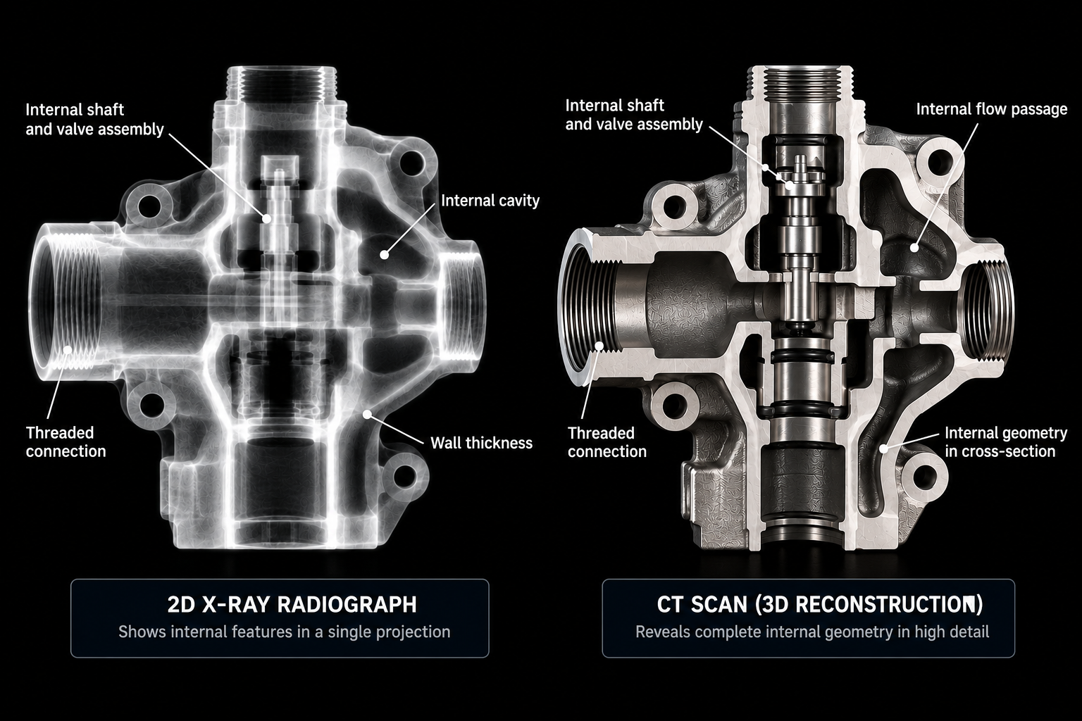
A Ball Grid Array package hides its solder connections underneath the die itself. There is no angle from which a camera, or even a standard 2D X-ray, can view a BGA joint without every other joint in the array overlapping it in the same projection. This single geometric fact is why micro-CT BGA inspection exists as a distinct discipline from general electronics X-ray inspection.
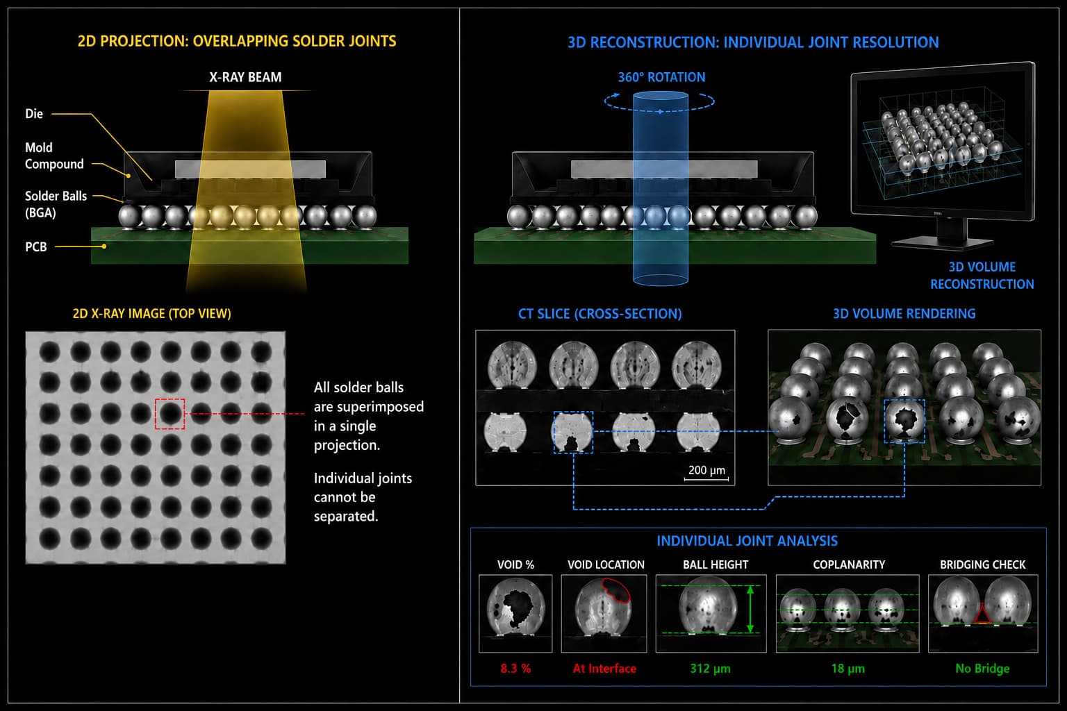
2D X-Ray vs. Micro-CT: BGA solder joints shown as overlapping projections in 2D X-ray and individually resolved with 3D Micro-CT reconstruction.
Why BGA Geometry Defeats 2D Inspection Methods
A 2D X-ray image is a flattened projection: every feature along the beam path is superimposed into a single plane. For a component like a connector or a discrete resistor, this is rarely a problem. For a BGA package, it is a fundamental limitation, because the solder balls sit in a dense grid directly beneath the die, and a 2D projection collapses the entire grid into overlapping shadows. XRAY-LAB has documented this same overlap problem for dense electronic assemblies in detecting hidden assembly defects inside a smartphone, where components stacked at high density cannot be individually resolved without full volumetric reconstruction.
Micro-CT solves this by reconstructing the package as a 3D volume rather than a flat projection, so each solder ball can be isolated and examined individually rather than viewed as one indistinguishable shadow among hundreds.
What Solder Joint Inspection at This Scale Actually Measures
Solder joint inspection under micro-CT is not a visual pass or fail. It produces measurable data on each individual connection:
Measurement | What It Indicates |
Void percentage per ball | Thermal and mechanical reliability risk at that specific joint |
Void location within the joint | Whether voiding sits centrally (lower risk) or at the interface (higher risk of early failure) |
Ball height and coplanarity | Whether the package seated correctly during reflow |
This is PCB defect analysis at the level individual joints, not the board as a whole, which is why void detection on BGA packages requires resolution fine enough to separate a single ball from its immediate neighbors, often in the range of a few microns depending on ball pitch.
Resolution Requirements Scale With Package Density
As BGA pitch shrinks, and it continues to shrink across most electronics categories, the resolution needed to resolve individual joints tightens correspondingly. A package with a wide ball pitch can often be inspected reliably with the same electronics CT scanning setup used for general PCB assemblies. A fine-pitch package approaching chip-scale packaging density requires a purpose-built micro-focus system, the class of equipment XRAY-LAB details in its standard X-ray and CT systems catalogue, where compact high-precision systems are specifically positioned for microelectronics work distinct from larger casting or structural component inspection.
Reliability consequences of an undetected BGA void follow the same underlying failure pattern XRAY-LAB has outlined more broadly for electronics: a joint that passes electrical test at time of manufacture can still carry a void that becomes a fatigue crack under thermal cycling, the exact concern raised in why X-ray inspection is critical for electronics reliability.
XRAY-LAB performs micro-CT BGA inspection using systems and resolution settings matched to specific ball pitch and package density, delivering measurable void, height, and bridging data rather than a simple accept or reject image.
Frequently Asked Questions
What is micro-CT BGA inspection?
It is the use of high-resolution industrial CT to reconstruct a BGA package in three dimensions, allowing individual solder joints to be examined separately rather than as an overlapping 2D projection.
Why can standard 2D X-ray not reliably inspect BGA solder joints?
Because the solder balls sit in a dense grid directly beneath the die, and a 2D projection superimposes every ball’s shadow into a single flat image.
What does solder joint inspection measure on a BGA package?
Void percentage and location per ball, ball height and coplanarity, and bridging between adjacent balls.
Does electronics CT scanning need different equipment for fine-pitch BGA packages?
Often yes. Wide-pitch packages can use general-purpose electronics CT systems, while fine-pitch or chip-scale packages typically require a micro-focus system built for higher resolution.
Why does void detection at the joint level matter if the board passes electrical test?
A joint can function correctly at the time of test while still carrying a void that develops into a fatigue crack under later thermal cycling, causing a field failure.