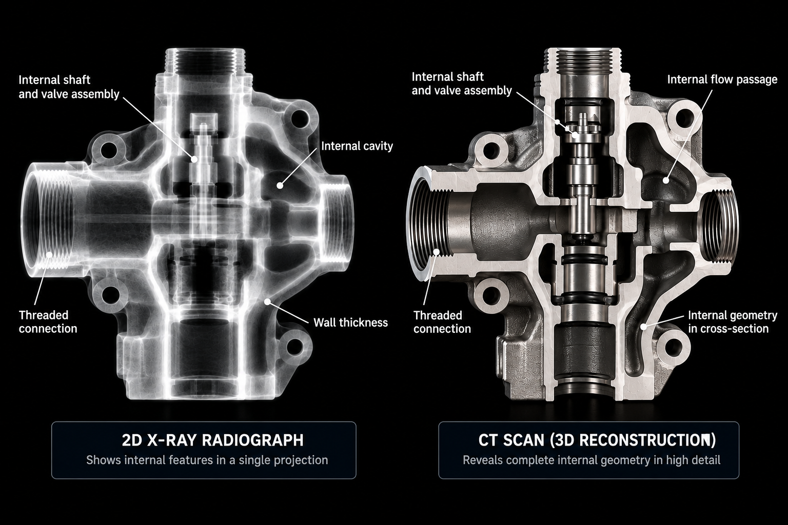
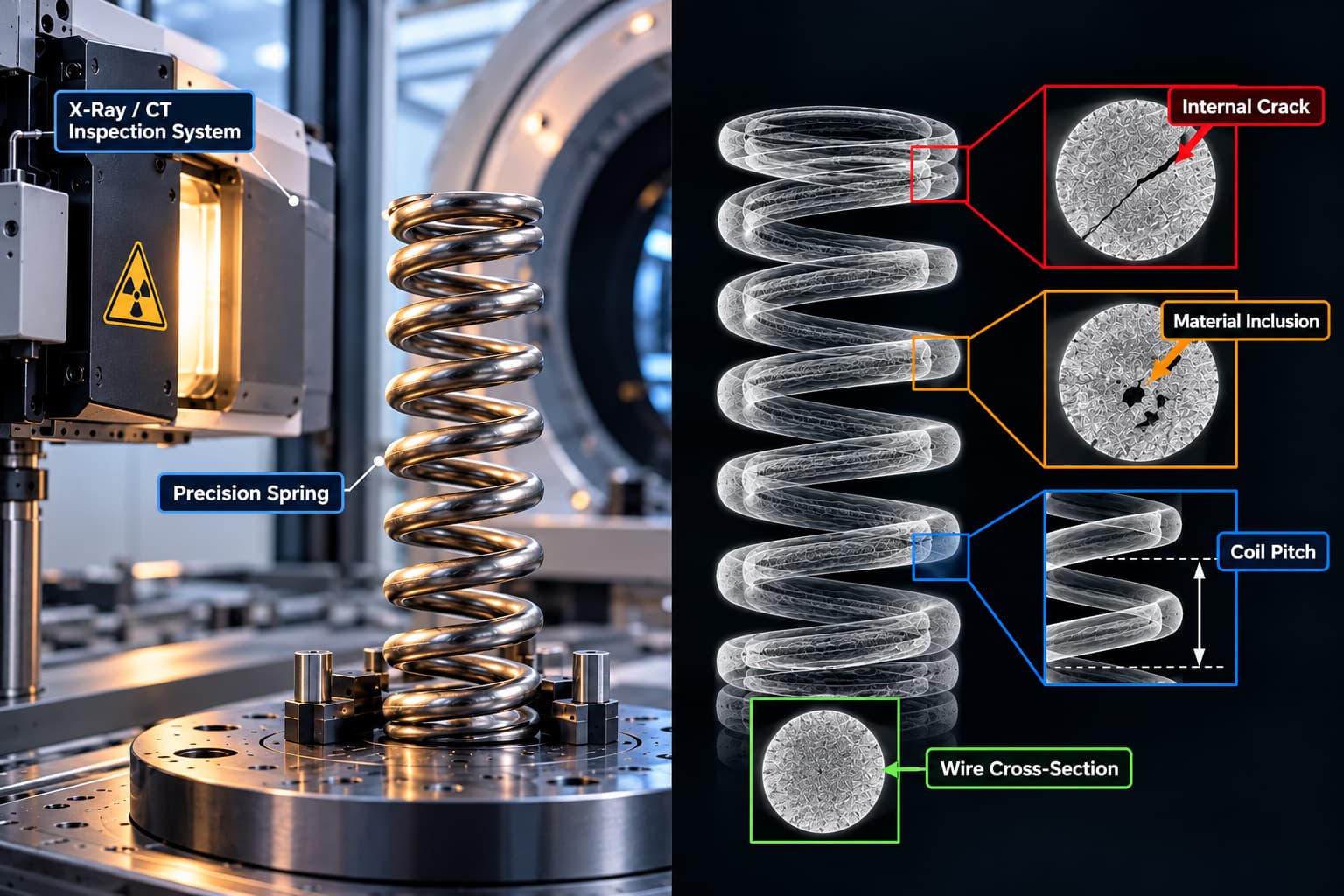
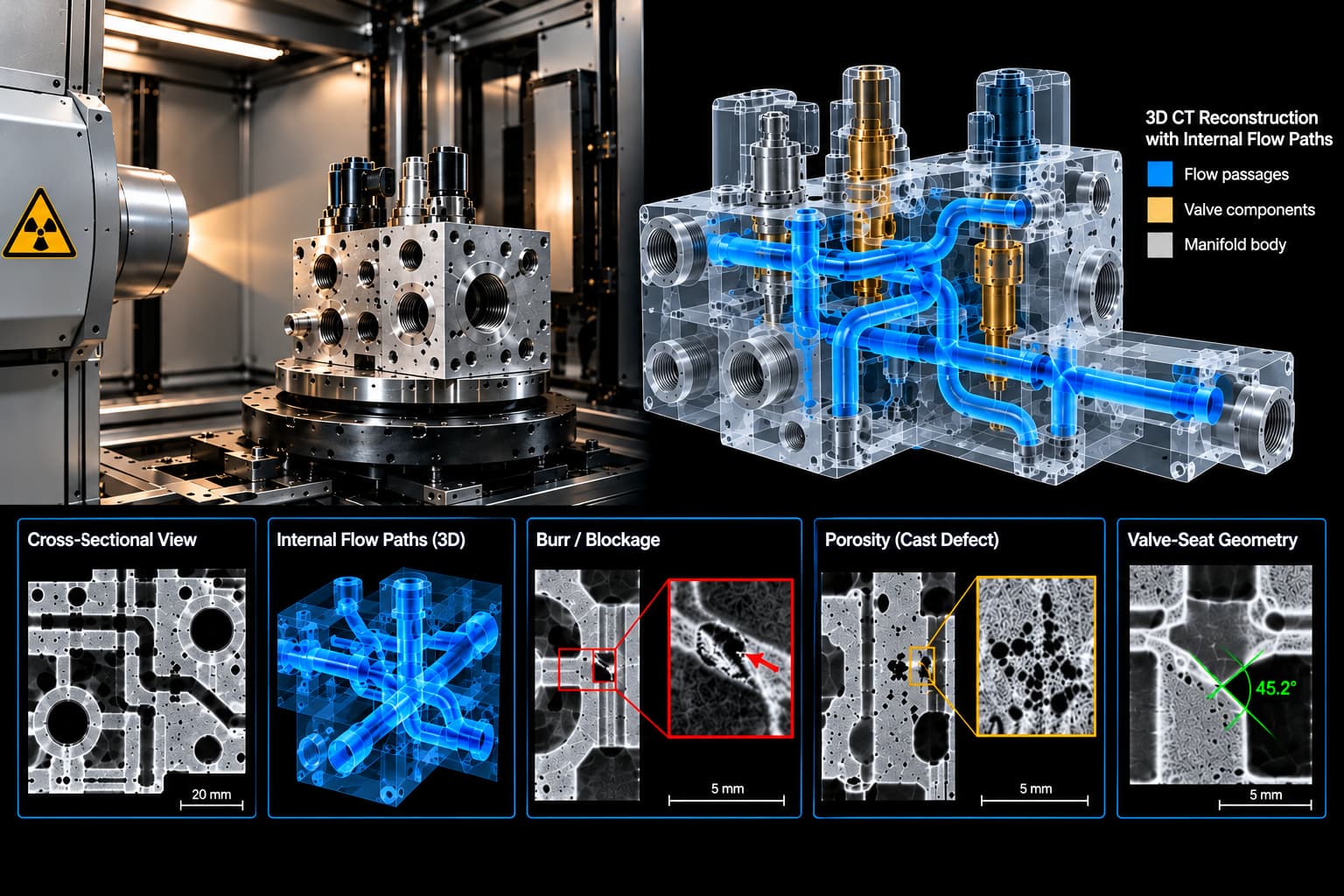
A connector’s job looks simple from the outside: two surfaces meet, and current flows. What determines whether that connection stays reliable over years of thermal cycling and mechanical stress happens entirely inside the housing, at the pin, the crimp, and the solder or press-fit joint, none of which a visual inspection or a continuity test can fully verify.
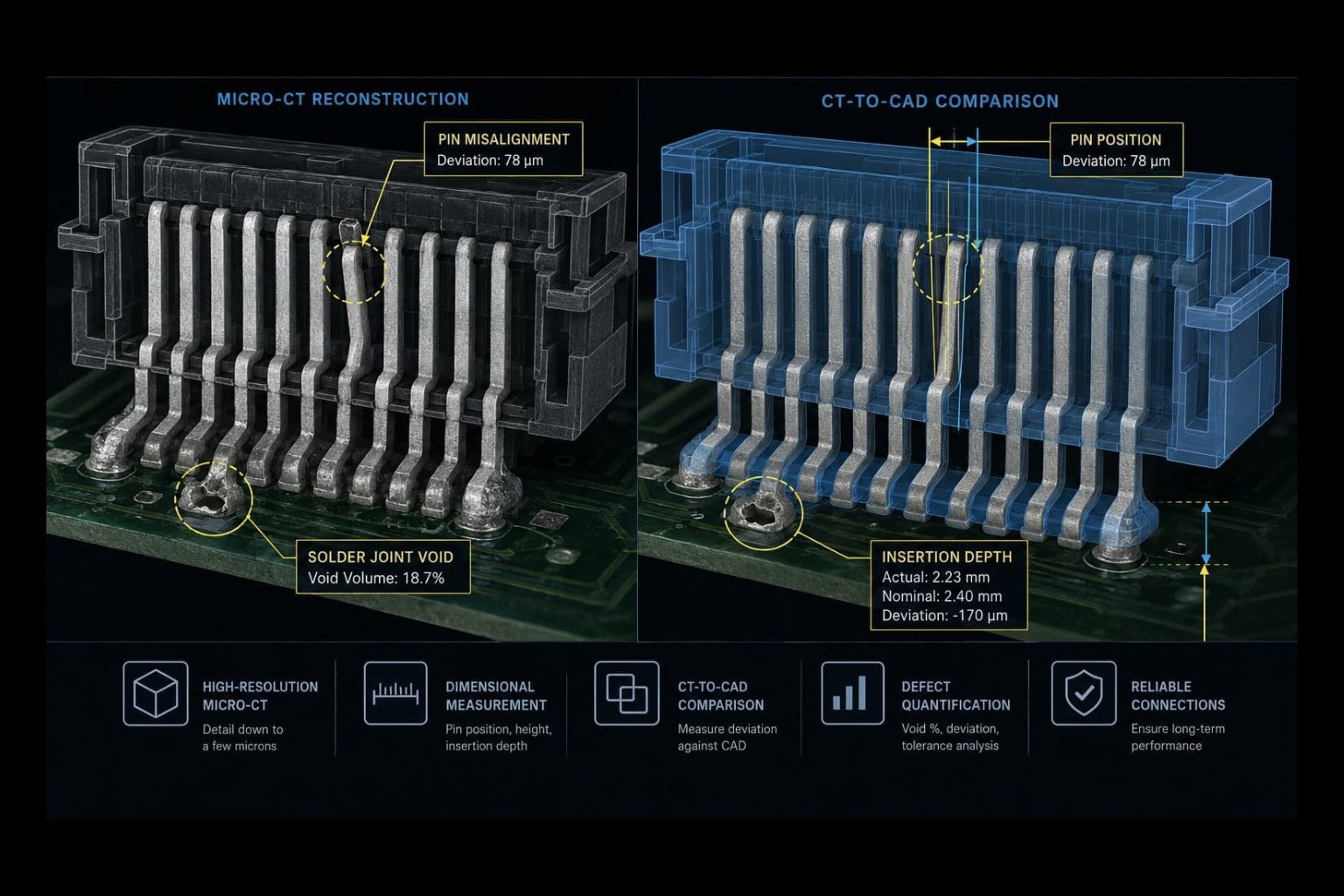
Micro-CT and CT-to-CAD analysis revealing hidden PCB connector defects and dimensional deviations.
Three connector failure points micro-CT routinely uncovers:
- Pin misalignment or deformation. A bent or off-axis pin can still make contact and pass an initial electrical test, while carrying reduced contact surface area that degrades under vibration or repeated mating cycles.
- Crimp or press-fit voids. Gaps inside a crimped connection reduce the effective contact area and increase localized resistance, a defect invisible from outside the crimp barrel.
- Solder joint voiding at the connector-to-board interface. The same void mechanism that affects BGA packages applies at connector solder joints, where a partially voided joint can pass functional test and fail months later under thermal stress.
Why PCB Connector CT Inspection Requires Dimensional Precision, Not Just Imaging
PCB connector CT inspection differs from general defect screening in one important way: much of what matters is dimensional, not just visual. Pin position, contact surface flatness, and insertion depth are measurable tolerances, not simply present-or-absent defects. Electronic component analysis at this level compares the CT-reconstructed geometry directly against the CAD model, the same CT-to-CAD comparison workflow XRAY-LAB uses for other precision components in its CT-to-3D model reconstruction process, applied here to pin geometry instead of a mechanical part.
Connector Defect | Consequence If Undetected | What Micro-CT Measures |
Pin misalignment | Reduced contact area, intermittent connection under vibration | Pin position vs. CAD, deviation in microns |
Crimp/press-fit void | Elevated resistance, localized heating | Void percentage within crimp barrel |
Solder joint void at connector base | Fatigue crack risk under thermal cycling | Void percentage and location per joint |
Insertion depth deviation | Incomplete mating, contact resistance instability | Depth measurement against design tolerance |
Where This Fits Into Production-Line Quality Control
Connector defect detection is most valuable when it happens consistently across a production run rather than as an occasional spot check, since connector defects frequently trace back to a specific crimping tool, a solder profile drift, or a supplier batch rather than occurring randomly. This is the same continuous-monitoring logic XRAY-LAB applies through inline scanning, detailed in how XRAY-LAB powers smart production with real-time inspection, where defects as small as 50 to 100 microns are caught before they propagate through a full batch.
PCB quality inspection programs that treat connectors as a secondary concern behind the board itself tend to miss this pattern, since a connector failure often surfaces as an intermittent field complaint long after the board itself has been cleared of blame, echoing the broader reliability argument XRAY-LAB has made in why X-ray inspection is critical for electronics reliability.
XRAY-LAB performs micro-CT electronics inspection on connectors using resolution and CT-to-CAD comparison workflows suited to each connector’s pin pitch and geometry, giving manufacturers measurable pass or fail data rather than a visual judgment call.
Frequently Asked Questions
What is PCB connector CT inspection?
It is the use of high-resolution industrial CT to examine a connector’s internal geometry, pin alignment, crimp integrity, and solder joints, and compare the result against CAD tolerances.
Can micro-CT electronics inspection detect pin misalignment that still passes an electrical test?
Yes. A misaligned pin can still complete an electrical circuit while having reduced contact area, a risk that only dimensional CT measurement reveals.
How does connector defect detection identify crimp voids?
By measuring void percentage inside the crimp barrel from CT reconstruction, since a crimp void is not visible externally and does not always affect initial continuity testing.
Why is PCB quality inspection often incomplete without connector-level checks?
Because connector-related field failures frequently appear as intermittent issues traced back well after the board itself has been ruled out, once the actual defect origin is inside the connector.
Does electronic component analysis use the same CT setup for all connector types?
No. Resolution and scan parameters are matched to pin pitch and connector geometry, since fine-pitch connectors require finer resolution than larger, widely spaced designs.