Contemporary cellphones frequently pass final production testing with no discernible performance problems. However, internal assembly flaws that go unnoticed during traditional quality inspection and only show up after the product is delivered to the client are the root cause of many device failures.
These failures are frequently the result of minor internal flaws like weak solder joints, misaligned flex cables, insufficient bonding, or inconsistent structural assembly rather than significant manufacturing mistakes. Conventional inspection techniques are restricted to surface-level testing and are unable to assess interior assembly integrity since smartphones are extremely small and sealed devices.
Defects concealed during manufacturing can lead to warranty claims, product returns, and customer unhappiness, which poses a serious problem for manufacturers.
By producing a comprehensive three-dimensional view of a smartphone’s internal assembly without causing any harm to the device, industrial CT scanning overcomes this restriction. This enables manufacturers to find structural anomalies that are missed by conventional inspection systems, check assembly accuracy, and find hidden flaws early.
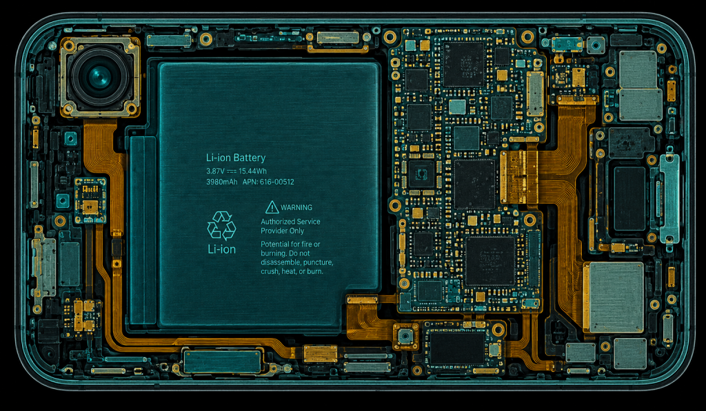
Full internal CT panoramic slice of a smartphone in false-color teal/amber palette showing battery, PCB, flex cables and camera module simultaneously
What Current Inspection Methods Can and Cannot See
In terms of resistance to inspection, the modern smartphone is unsurpassed amongst any mass-produced consumer goods. The sealed design, high-density packaging of components, and mixed-material composition render smartphones resistant to any of the traditional forms of inspection, not because of some inadequacy of these approaches, but because of their design.
Below is a brief explanation of what each inspection approach can and cannot see for the five essential areas in smartphone manufacture:
Inspection Target | Visual Inspection | AOI | 2D X-ray | Industrial CT |
Battery integrity & bond | ✗ | ✗ | ✗ | ✓ |
Flex cable routing & damage | ✗ | ✗ | Partial | ✓ |
Camera module alignment | ✗ | Partial | ✗ | ✓ |
BGA solder joint quality | ✗ | ✗ | Partial | ✓ |
Inter-component clearances | ✗ | ✗ | ✗ | ✓ |
Both visual inspection and AOI testing have their scope confined to surface-level testing. This makes them suitable for use on the production line but unable to identify defects that are not visible on the outside. Although 2D X-ray testing allows for better visibility compared to visual inspection and AOI testing, it may be hard to distinguish the defects in highly complex smartphone configurations due to the overlapping components in the projected image.
Industrial CT offers a distinct edge in this situation. It enables for comprehensive inspection without changing or harming the sample, travels through sealed housings, and reconstructs the entire internal structure in three dimensions.
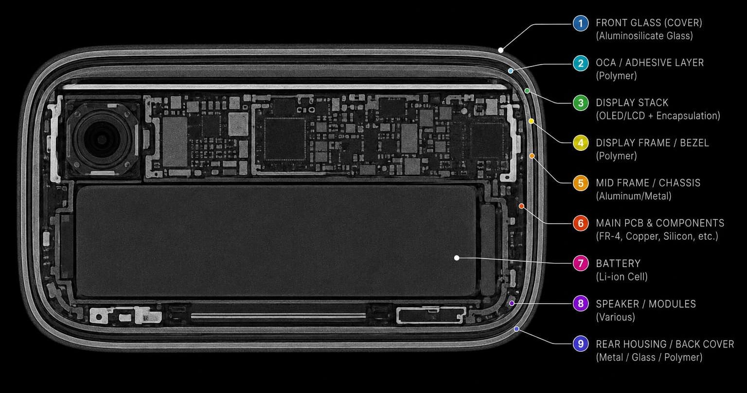
CT axial slice showing smartphone layer stack annotated from glass to rear housing
Five Assembly Defects That Only CT Scanning Catches
1. Battery Delamination and Adhesive Void Issues
In a smartphone today, the battery is bonded to the casing via an adhesive which not only serves as a mechanical anchor but is also critical in ensuring thermal contact between the battery and the housing casing. If the adhesive does not entirely bond to the battery surface during production, the anchoring is compromised.
During regular use, such as charging cycles, temperature change, and even incidental drops, the under-anchored battery will move inside the phone. Such movement leads to accelerated electrode degradation. As the electrodes degrade, gas is created, leading to swelling.
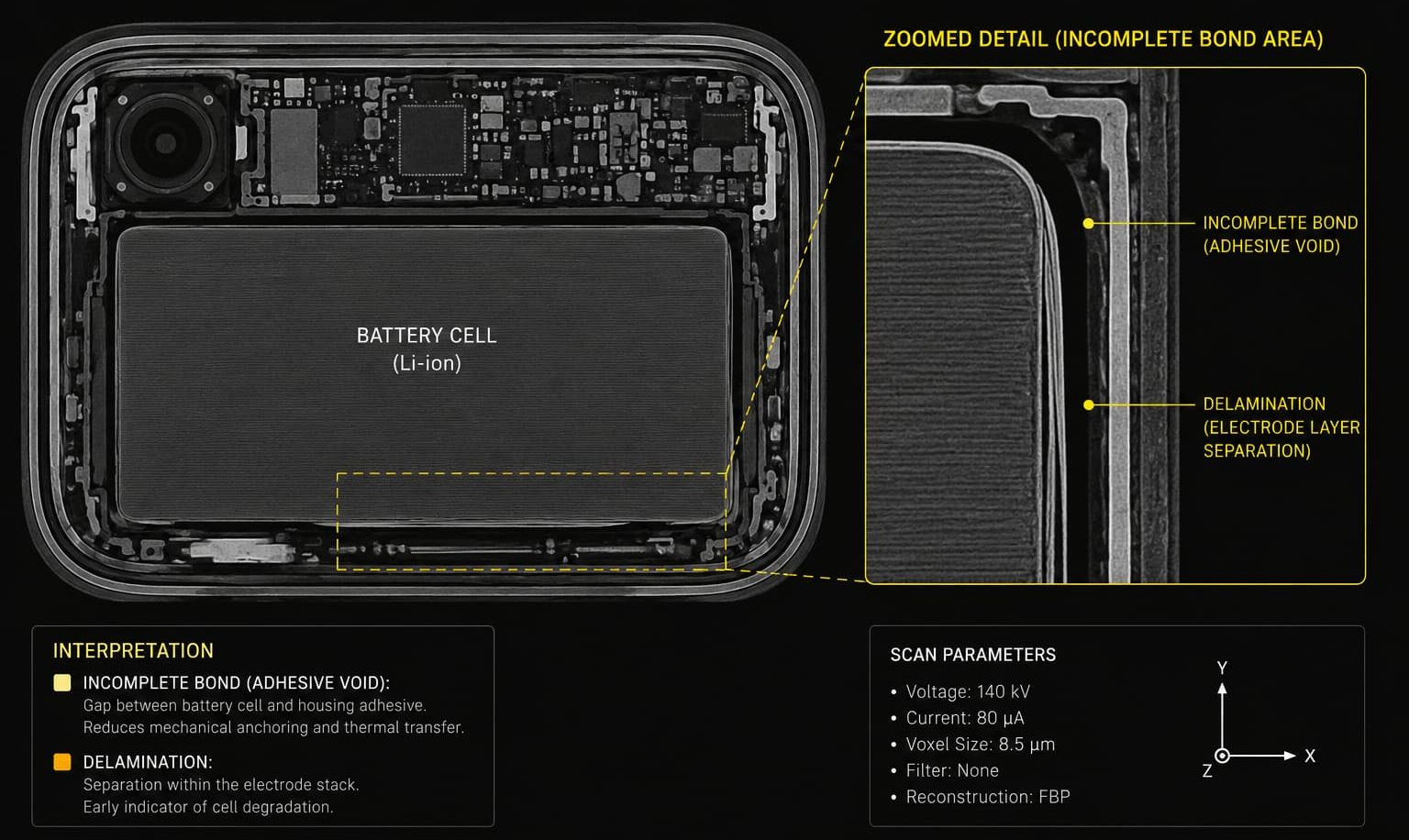
CT slice through battery layer with incomplete bond area and delamination callout
2. Flex Cable Distortion & Routing Errors
A flex cable is the connecting element of a smartphone-it is a thin foldable conductive ribbon that connects the display, camera, switches and charging system with the main printed circuit board. The way a flex cable routes inside the housing is carefully thought out and deliberate. If this routing path is not adhered to, the flex cable is subjected to stress right from the start once the housing is closed.
The reason is that when a flex cable is distorted or crushed between two parts, there is no immediate damage or malfunction. It would still be working perfectly fine at first and even pass all electrical tests. But after a while it would break down gradually due to combined effects of heat and mechanical pressure in ways that make it extremely hard to simulate outside the phone.
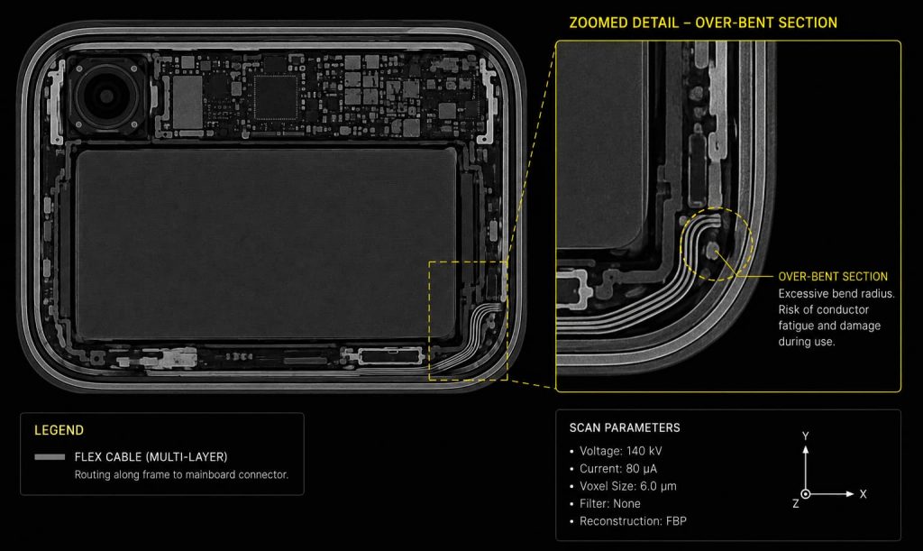
CT slice showing flex cable routing with over-bent section highlighted
3. Camera Module Positioning Errors
In today’s smartphones, the cameras used are sophisticated optical devices. The amount by which the camera module needs to be positioned to produce quality results is very small. Even a tiny displacement that a person cannot see or feel makes a difference in the image produced.
Positioning errors show themselves blurring at the edges of the frame, autofocus problems, and optical image stabilization issues. The customer sees it. They get a replacement camera module from the service center without understanding what the underlying issue is.
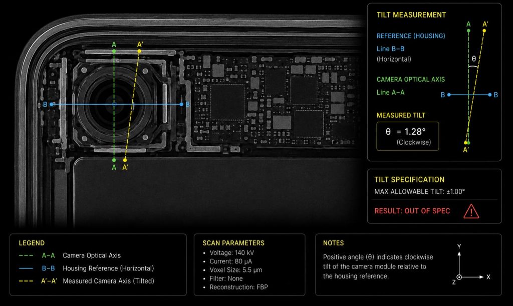
CT slice with camera module tilt measurement overlay
4. Quality of BGA Solder Joints
Most advanced components of a smartphone such as Application Processor, Memory, and Power Management Unit are soldered to the Printed Circuit Board via arrays of small solder balls located in a grid underneath each component’s body. Those joints are completely covered by the component body and are not detectable via AOI. Standard X-Ray technology overlays them at this density. Electrical Testing will give good results for a defective joint as long as it’s electrically continuous.
Solder void – the air bubble within a solder joint – lowers its capability to dissipate heat energy and resist mechanical loads. Small voids can be tolerated but larger voids or groups of them form a joint which will be susceptible to failure under thermal cycles of each charging.
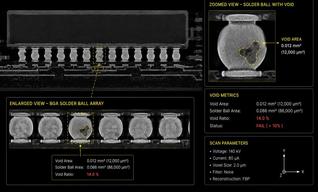
BGA solder void close-up with void area highlighted and measurement callout
5. Clearance Between Components Violation
This is such a crowded assembly; the spacing between two consecutive components cannot be arbitrary. The gap allowed between them has to be defined, and that spacing serves a very important purpose. When a product goes through the curing and reflow processes, this spacing becomes less.
The violation in clearance does not cause an instant failure but will eventually lead to a gradual problem. This would mean that the performance of the antennas will be affected due to proximity or shortened lifetimes because of thermal limitations or direct contact between the battery and PCB due to drop testing.
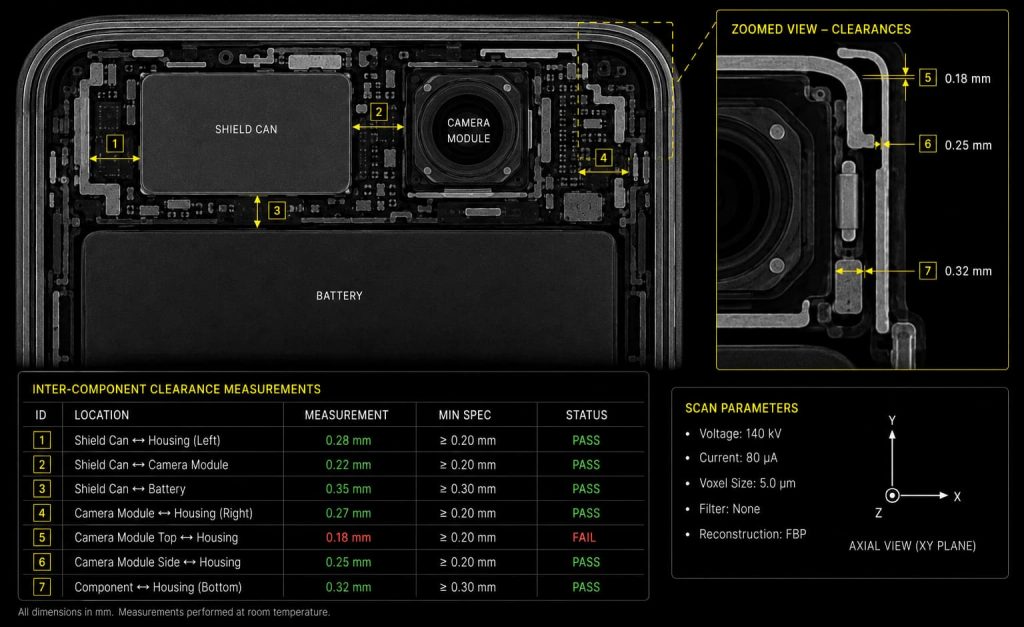
CT slice with inter-component clearance dimension callouts
Inspection technology that can examine intricate internal structures without physically opening the device is necessary to find internal smartphone assembly flaws. Incomplete adhesive bonding in battery cells, internal gas formation, electrode delamination, flex cable distortions, microscopic tears, camera module misalignment across multiple axes, excessive solder voids in high-density circuit boards, and incorrect component clearances are just a few of the critical defects that XRAY-LAB assists manufacturers in identifying through advanced industrial CT scanning. Engineering teams may track recurrent production anomalies, pinpoint defective units early, and enhance process reliability before hidden flaws cause field failures or expensive recalls because of XRAY-LAB’s accurate three-dimensional internal mapping.
What XRAY-LAB Finds — and What It Changes
During smartphone inspection, XRAY-LAB commonly detects recurring defects such as excessive solder voids in high-power components and improper flex cable positioning — issues that often remain invisible during conventional testing.
Beyond defect detection, CT analysis supports supplier quality validation by helping manufacturers trace recurring assembly issues back to their source and address process inconsistencies early.
As smartphones become more compact and internally complex, traditional inspection methods are increasingly limited in detecting hidden defects within sealed assemblies. Faster development cycles and higher component density demand more advanced inspection capabilities.
Industrial CT scanning addresses this challenge by providing non-destructive, three-dimensional visibility into fully assembled devices, allowing manufacturers to identify hidden defects directly during production rather than after product failure.
To improve assembly validation and prevent costly field failures, manufacturers can leverage XRAY-LAB’s industrial CT scanning solutions for deeper internal inspection and faster defect investigation.
Frequently Asked Questions
Why do smartphone batteries swell and how can CT inspection prevent it?
Battery swelling is caused by internal gas build-up from electrode delamination or electrolyte issues, defects present from the point of manufacture. CT scanning detects these conditions before the device ships, giving manufacturers the data to reject affected units and identify the assembly process root cause.
What does a BGA solder void look like on a CT scan?
On a CT slice, a solder void appears as a dark region within an otherwise solid solder joint, an air pocket where solder should be. CT measures the void’s size and calculates the void content per joint, which is compared against acceptance criteria to determine whether the joint meets specification.
Can CT scanning detect flex cable damage without opening the smartphone?
Yes. CT maps the complete routing path of every flex cable inside a sealed device, identifying over-bent sections, pinched areas, and micro-tears that produce no external symptom until the device fails under operational stress.
How accurate is CT scanning for camera module alignment in smartphones?
Industrial CT measures camera module position, tilt, lateral offset, and Z-axis height, to micron-level accuracy, well within the tolerance range that affects optical performance. It is the most reliable method for camera alignment verification in sealed assemblies.
How does smartphone CT inspection differ from standard X-ray inspection?
Standard 2D X-ray produces a flat projection where components overlap, useful for a broad overview but unable to isolate individual features at smartphone density. CT builds a full 3D volumetric dataset, allowing engineers to examine any layer, measure any dimension, and identify any defect in three dimensions-without destroying the device.