USB connectors are among the most widely manufactured electronic components, yet they are often inadequately inspected. From the outside, everything looks good; there are no holes in the casing; no bent pins are visible, and it passes the initial continuity test. However, there could be one bent pin, misaligned contacts, and even a hairline fracture in the overmolding making the connector useless
CT scanning offers a level of visibility for connector inspections that traditional inspection techniques cannot match. Manufacturers can use completely volumetric, non-destructive 3D imaging to find internal flaws and structural irregularities that would normally go undetected without destructive testing.
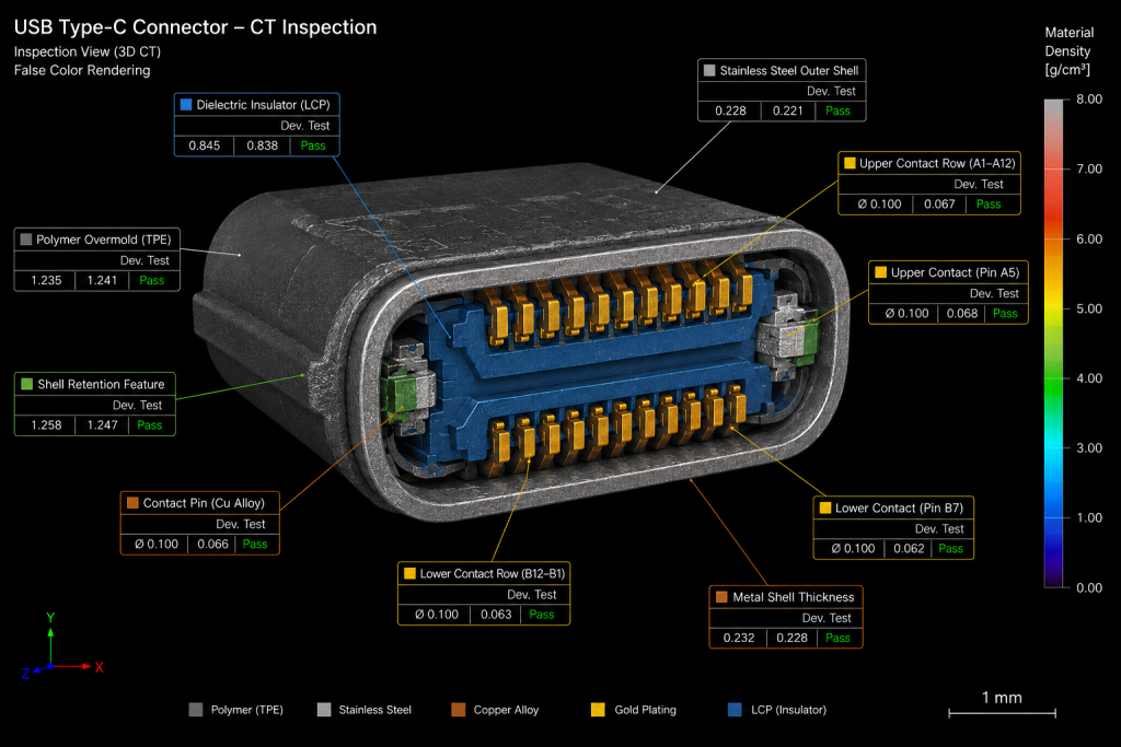
CT scan cross-section of a USB-C connector showing the internal pin array embedded in polymer housing
Common USB Connector Failures
USB connectors fail in predictable ways, most of which originate in manufacturing rather than field use. The most frequently observed failure modes include:
Pin misalignment and positional deviation. Individual signal and power pins must be held within micron-level tolerances to mate correctly with a receptacle. Even slight angular deflection, sometimes less than 0.5°, can cause intermittent contact, increased resistance, or complete mating failure.
Bent or deformed pins. Pins can be deformed during insert molding, during assembly of the connector into a PCB or harness, or during handling. A pin that appears straight from the exterior may be bent within the plastic housing where it cannot be seen.
Overmold cracking and voids. The plastic housing encapsulates the pin array and provides mechanical retention. Internal voids, sink marks, or stress cracks in the over mold can reduce pull-out strength and create failure points under vibration or thermal cycling.
Solder joint defects. In board-mounted USB connectors, CT reveals incomplete solder joints, bridging between adjacent pins, or lifted pads-all invisible from outside the connector.
Foreign material inclusion. Metal particles or flash from the stamping process can become trapped inside a connector housing during assembly, creating short-circuit risk.
Bent Pins and Hidden Deformation: Why Surface Inspection Misses Them
One of the major difficulties involved in testing USB connectors is the fact that the most important geometric aspects of the connectors are internal. The pin contacts are encased in plastic material, and the test must include more than just the measurement of positions, but also the proper orientation of the pins.
Optical inspection using magnifying cameras or structured light can measure the positions of pin tips and their surfaces. They cannot, however, determine whether a pin is bent, angled, or straight based on what they can see. A pin that appears to have a good position in the image may very well be angled or bent at its base in the mold-a flaw that will only become apparent when force is applied to mate with another connector.
Industrial computed tomography inspects the whole connector as an assembly, imaging it as a three-dimensional structure. This allows the positions, angles, and straightness of all the pins to be inspected separately over their entire submerged length. Any deviation from the desired geometry can be automatically detected by inspection software.
When hidden connector defects do reach the field, CT is the fastest path to a definitive answer. Read more: How CT Scanning Accelerates Root Cause Failure Investigations
Assembly Verification with CT
The CT examination of USB connectors does not only entail finding defects in the components. Instead, it ensures that all the internal features of the component are correctly placed and in good tolerance.
Typical verification tasks include:
- Pin pitch measurement-verifying that center-to-center distances between adjacent pins match the design specification across the full array
- Perpendicularity checks-confirming that each pin is perpendicular to the mating face within allowable angular tolerance
- Housing wall thickness-ensuring that the overmold maintains minimum wall thickness between pin cavities to prevent punch-through under insertion force
- Insert depth-verifying that terminal contacts are fully seated at their correct depth inside the housing, especially for board-mounted press-fit variants
This kind of volumetric verification cannot be achieved with any surface-based or contact measurement method on an assembled connector.
CT vs. Optical Inspection for Connectors
| Capability | Optical / Vision Systems | Industrial CT Scanning |
| Surface defect detection | ✅ Excellent | ✅ Good |
| Pin tip position | ✅ Yes | ✅ Yes |
| Pin angle / straightness (full length) | ❌ Not visible | ✅ Full 3D measurement |
| Overmold void detection | ❌ No | ✅ Yes |
| Solder joint inspection | ❌ No (hidden) | ✅ Yes |
| Foreign material detection | ❌ Limited | ✅ Yes |
| Assembly completeness verification | ❌ Partial | ✅ Full volumetric |
| Destructive to part | ❌ No | ❌ No |
| Speed | ✅ Fast (inline capable) | ⚠️ Slower (batch/offline) |
Optical systems remain valuable for high-speed, surface-level screening in production lines. CT is the appropriate tool for qualification, failure analysis, and process validation — situations where the internal condition of the connector is what needs to be understood.
Applications: Automotive and Consumer Electronics
USB connectors have seen fast adoption within the automotive industry due to the increased usage of infotainment systems, EV chargers, and advanced in-car electronics. For automotive applications, USB connectors must withstand vibrations, temperature cycles from −40°C to +125°C, and last more than 15 years.
As for automotive connectors, CT inspection can be applied within PPAP and first article inspection processes to confirm that the connector complies with its internal dimensions prior to manufacturing. CT data can be used for design evaluation, supplier certification, and process validation, thus providing objective information about internal dimensions of every certified design.
For consumer electronics, the problem becomes one of volume and miniaturization. The USB-C connector, which has replaced the Micro-USB and Type-A connector on most modern devices, features 24 pins in a connector that is smaller than the size of a fingernail. At this level of miniaturization, even a pin misalignment of 50 microns can become an issue.
The CT process is used in consumer electronics for supplier qualification, incoming lot inspection of high-volume connectors, and failure analysis of connector problems revealed by field returns. A root cause analysis, which might otherwise take many destructive sections on many samples, can now be done without destruction on the actual failed samples.
USB connectors are one piece of the puzzle. See how CT inspection applies across the full smartphone assembly.
Conclusion
The USB connector is a compact, affordable, and common component, and those attributes ensure that it is never tested internally. Optical test methods assure engineers about what they can see, while CT test methods assure them everything they cannot.
For connector engineers in automotive connector supply chains, or quality teams tasked with ensuring the reliability of USB-C connectors used in large-scale consumer electronic devices, the difference between a pass on the optical side and a fail detected by CT is precisely where field failure occurs. Bent pins passing a go/no-go gage test, non-conductive voids within the connectors, or soldering defects that pass through a single thermal cycle but not a hundred thermal cycles are only found by CT inspection.
Why Manufacturers Choose XRAY-LAB for Connector Inspection
The XRAY LAB is equipped with cutting-edge micro and nano-focus CT units, which provide a capability to analyze the internal structure of connectors down to a voxel size of 1 micron, making it possible to visualize pins’ geometry, wall thickness, and solder joints in USB-C and other fine pitch connectors.
Every inspection is supported by experienced NDT engineers who interpret CT data in the context of your manufacturing process, acceptance criteria, and application requirements. XRAY-LAB serves manufacturers across the automotive, aerospace, medical device, and consumer electronics sectors from its inspection facilities in the USA.
Contact XRAY LAB to discuss your connector inspection requirements
Frequently Asked Questions
What resolution is needed to inspect USB connector pins with CT?
Microfocus CT systems with voxel resolutions of 5–20 microns are typically used for USB connector inspection.
At this resolution, individual pin geometry, solder joint quality, and overmold structure are clearly resolvable.
Nanofocus systems (sub-micron resolution) are used for the smallest USB-C and fine-pitch connector variants.
Can CT detect failures that pass functional electrical testing?
Yes, this is one of CT’s most important applications for connectors.
A slightly bent pin may still make electrical contact under normal mating force while failing to meet positional tolerance.
CT identifies these marginal conditions before they become field failures under vibration or repeated mate/unmate cycles.
How long does a CT inspection take for a USB connector?
A typical acquisition and reconstruction for a single USB connector takes between 5 and 20 minutes depending on the required resolution and scan volume.
Automated software analysis and report generation can follow immediately. For batch inspection, multiple connectors can be scanned simultaneously.
Is CT suitable for 100% inspection of high-volume connector production?
Standard CT is not inline-capable for typical production volumes. It is best used for first-article, lot auditing, and failure analysis.
However, inline CT systems do exist for selected applications where quality criticality justifies the investment.