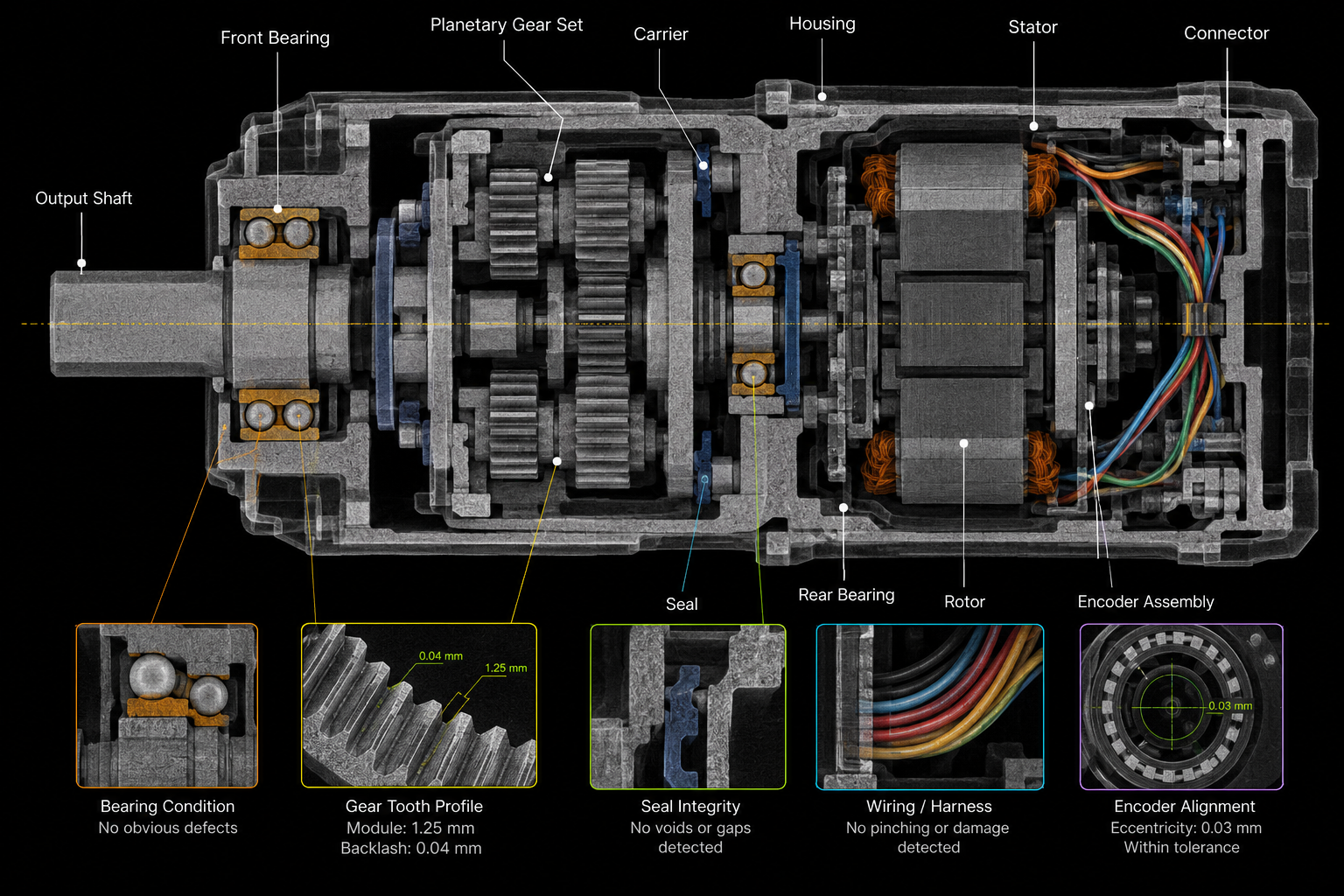
EV power modules convert battery DC to motor-driving AC through IGBT or SiC dies soldered to a ceramic substrate, which is soldered again to a copper baseplate. These solder layers, often under 100 microns thick, are the primary heat path out of the die. A void inside that layer is not cosmetic. It is a thermal defect that grows under load, which is what makes power electronics inspection fundamentally different from standard PCB inspection: the failure path is thermal, not just electrical.
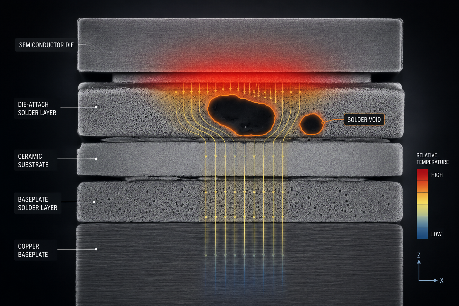
Conceptual diagram of an EV power module cross-section, showing a solder void in the die-attach layer disrupting the heat path from the semiconductor die to the copper baseplate.
A solder void is a trapped gas pocket, usually from flux outgassing during reflow. It blocks heat flow locally, so the die runs hotter than intended in that spot. Every drive cycle then subjects the void’s edge to thermal expansion and contraction, which slowly extends it into a crack. Once the crack network spans the joint, thermal resistance rises sharply and the die overheats under normal load. The mechanism mirrors what XRAY-LAB has documented in lithium-ion cells prone to internal short circuits: a defect sealed inside a working component, invisible until it has already progressed.
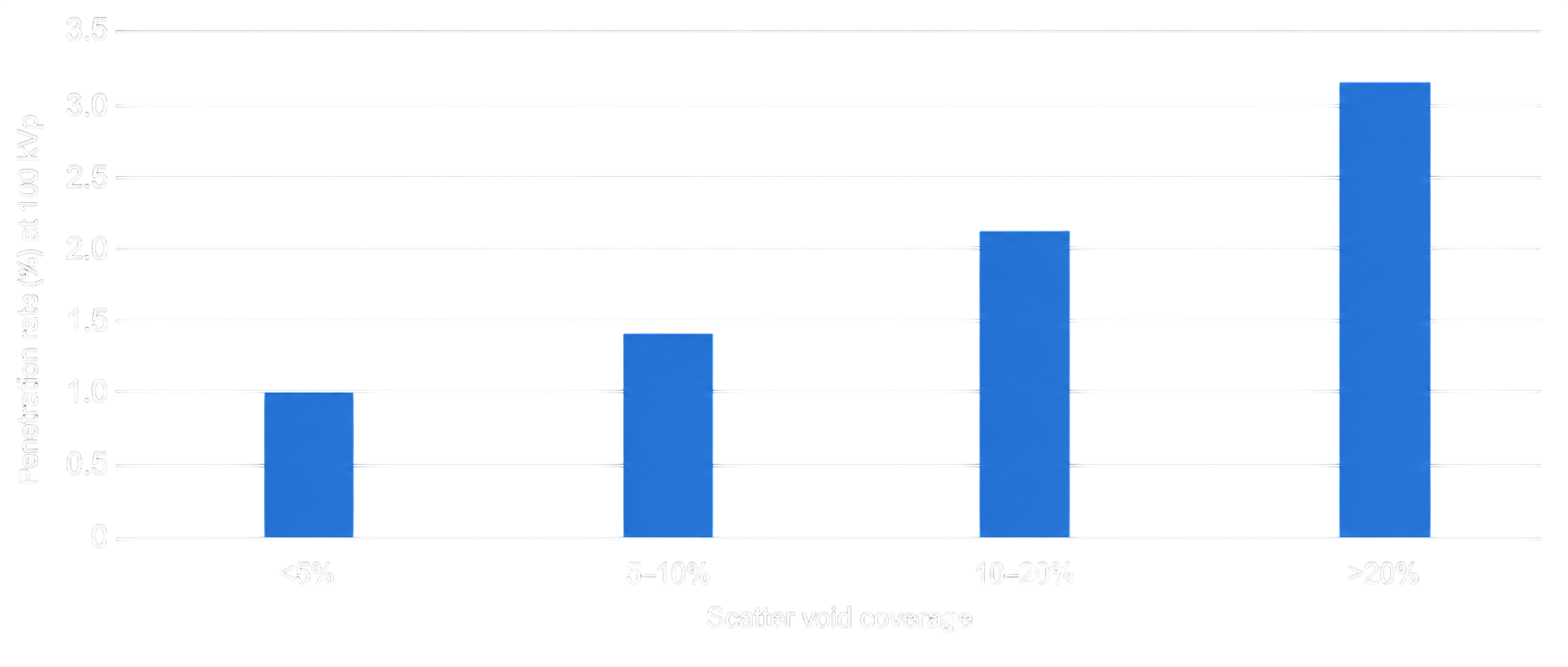
Relative thermal resistance increases as solder void coverage grows within the die-attach layer, with risk accelerating once voids exceed approximately 10% of joint area. Illustrative engineering relationship, not measured data; actual thresholds vary by module design and duty cycle.
The chart above shows the general shape of this relationship: thermal resistance does not increase linearly with void coverage, it accelerates once voids exceed roughly 10% of joint area, which is why early-stage solder void detection matters more than end-of-line functional testing.
A module can pass electrical test today and still carry a void that fails it in a year. Functional test checks whether the module works at that moment; it cannot see a partially voided joint that hasn’t yet crossed a performance threshold. Cross-sectioning can see the void, but only in one plane, and it destroys the part. X-ray inspection for EV modules avoids both limits. 2D/2.5D X-ray produces a density map of the full joint area in seconds; voids appear as lighter regions where less material blocks the beam. CT goes further, reconstructing the joint in three dimensions so void size, shape, and position can be measured rather than estimated by eye.
Method | View | Destructive | Best for |
Functional test | None (electrical only) | No | Confirming the module works today |
Cross-section | Single 2D plane | Yes | One-time deep dive on a known failure |
2D/2.5D X-ray | Full joint, top-down | No | Fast in-line void screening |
Industrial CT | Full joint, 3D | No | Precise void location and size for qualification |
Void detection depends on attenuation contrast: solder absorbs X-rays, voids (air) do not. The complication in a power module is the layer stack. Copper baseplate, solder, ceramic, solder, die: each layer attenuates differently, and beam hardening through the copper can distort contrast if exposure settings are borrowed from a generic recipe instead of tuned to this specific stack. XRAY-LAB covers this same physics in how X-rays behave inside dense metal and why it affects inspection accuracy. For power modules, correct voltage, current, and filtration settings are what make a void reading trustworthy rather than approximate.
A module with a moderate void percentage that passes final test is exactly the kind of defect that resurfaces later as warranty exposure. XRAY-LAB has shown how advanced X-ray inspection reduces warranty claims by catching internal defects before shipment. Solder void detection on power modules is a direct application: it converts an invisible reliability risk into a measurable, documented pass/fail decision at the point of manufacture.
XRAY-LAB performs EV power module CT inspection using 2D/2.5D X-ray for fast void screening and industrial CT when a joint needs full volumetric characterization, with exposure parameters set for each module’s specific material stack rather than a generic default. For manufacturers moving from qualification into volume production, the same inline CT capability scales this approach from prototype to production line.
Frequently Asked Questions
What is solder void detection in EV power module inspection?
It is the use of X-ray or CT imaging to find trapped gas pockets inside die-attach or baseplate solder, without cutting the part open.
How does X-ray inspection for EV modules differ from cross-sectioning?
It is non-destructive and images the full joint area, while cross-sectioning destroys the sample and only shows one slice.
What void percentage matters in power electronics inspection?
Many manufacturers flag concern once void coverage passes roughly 10 to 15% of joint area, though thresholds vary by module design and duty cycle.
Is semiconductor quality control different for power modules than for standard PCBs?
Yes. Power modules see higher current density and thermal cycling, so a small void can become a fatigue crack far faster than it would on a standard board.
Can EV power module CT inspection run on a production line?
Yes. 2D/2.5D X-ray handles fast in-line screening, and CT is used for detailed checks on flagged parts or scheduled sampling.