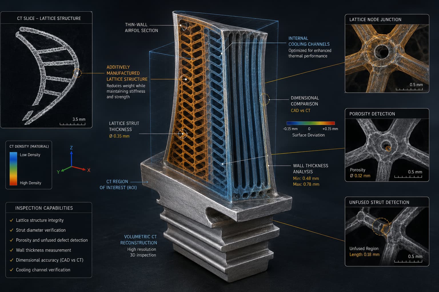
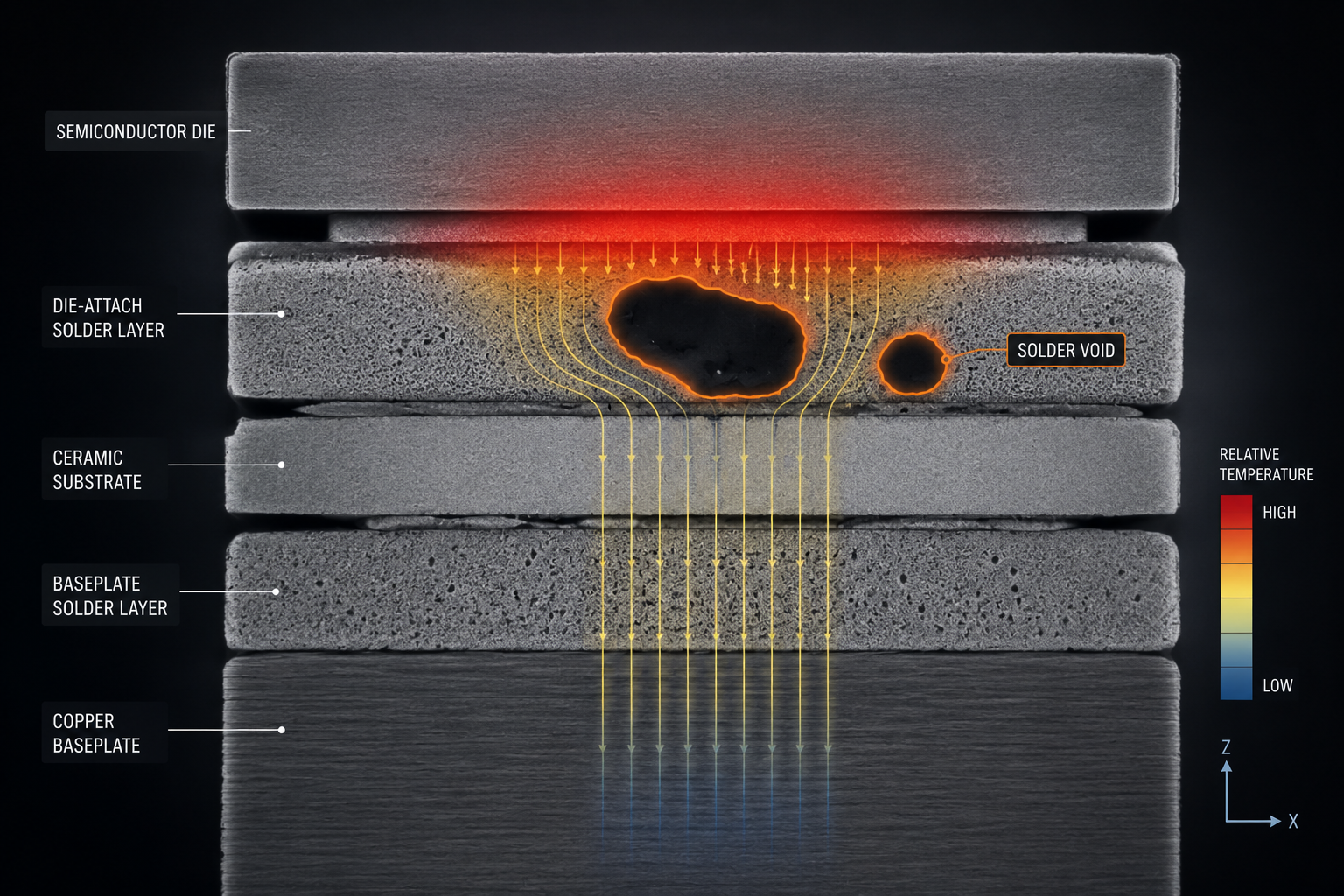
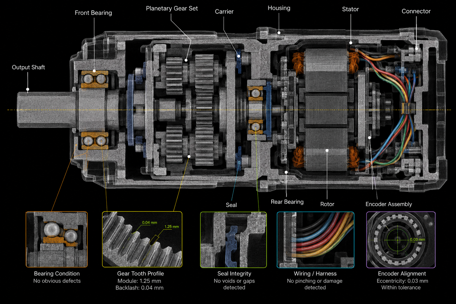
Have you ever asked yourself what exactly is in the charger sitting at your desk?
People do not care too much about power adapters. They need their devices charged, and if it works, nothing else matters. Yet when it comes to people designing and manufacturing these products, the question suddenly acquires another dimension.
While seemingly straightforward, a power adapter is a highly complicated product. Behind the walls of its plastic housing hides a transformer, PCB populated with numerous components; solder joints exposed to repeated thermal stress and potting material covering the whole ensemble together. Each and every one of these components can potentially contain defects invisible to any traditional method of checking.
This is exactly where Industrial Computed Tomography (CT) is needed.
Being a revolutionary technology in many ways, CT scanning creates an accurate 3D model of the interior of the adapter piece-by-piece, layer-by-layer, without breaking it or damaging the object. CT scanning is the only way to examine the inside of the component without opening or damaging it (Non-Destructive Testing), and with submicron accuracy.
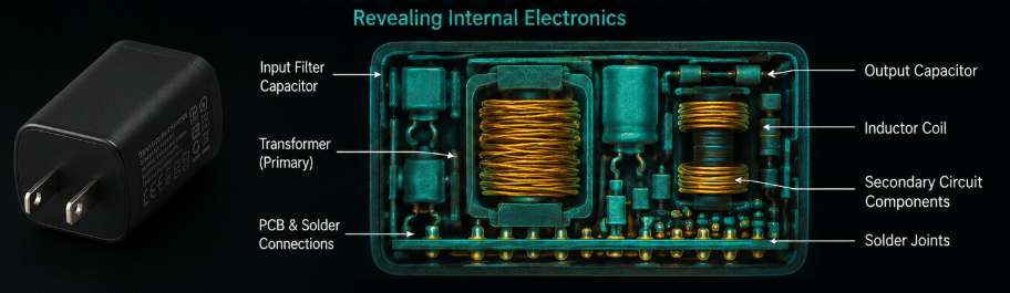
Industrial CT scan cross-section of a power adapter revealing internal electronics and solder joints.
Why Power Adapters Are the Perfect CT Subject
A power adapter may seem easy to evaluate based on its appearance, plastic case, a cord and a plug. However, in terms of engineering and quality, power adapters rank among the hardest items to check in any consumer electronics.
They are designed to be enclosed. While the potting compound used to protect electronics against humidity, vibration and heat will effectively shield the internal parts from moisture, it will also make visual examination impossible after assembling. After sealing, finding defects becomes very hard without the use of sophisticated systems.
They are subjected to constant stress. In each charge cycle, the components will undergo thermal expansion and contraction, making solder connections bend, the transformer heat up, PCB suffer micro-stresses, and so forth. Even something undetectable when the device was made can turn out to cause a malfunction months later.
The implications of such failures can be severe indeed. Power adapters with cracked solder joints, improperly aligned transformers, and voids within the potting material are not merely dysfunctional units – they represent fire hazards. The importance of the internal structure of power electronic devices connected to AC mains is being considered more than ever before by regulatory bodies.
But traditional methods of quality control were designed for other purposes.
2D X-ray offers a two-dimensional representation that allows for quick visualization; however, this method cannot detect defects hidden within overlapping parts and offers no depth data. AOI captures only the surface of the device. Destructive cross-sectioning can visualize one plane at a time – and requires destroying the object.
By contrast, industrial CT scanning does away with all three constraints. It provides three-dimensional images, allowing for viewing layers inside the sealed housing without damaging the test specimen, and enables re-testing the unit.
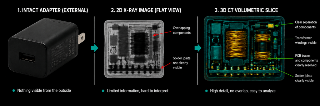
Side-by-side comparison photo — intact sealed adapter on the left, 2D X-ray flat image in the middle, 3D CT volumetric slice on the right.
5 Things Industrial CT Reveals Inside a Power Adapter
Here’s where the real value of CT scanning is used. The following are the five essential details that a CT scan will reveal a power adapter, information that will remain hidden from all other methods of inspection.
Internal Electronics Layout & Component Positioning
The CT system allows for a comprehensive 3D rendering of the inside of the adapter, including the placement of PCBs, component locations, and wiring. All these factors can be analyzed to ensure that everything has been put together according to specifications without having to open the adapter.
This information becomes crucial during first-article testing when introducing a new product.
Solder Joint Quality — Voids, Cold Joints & Bridging
The voids in a solder joint are quantified using CT in three dimensions, joint by joint. CT will also show cold joints and any solder bridging between the pads. It will highlight any void greater than the thresholds set in IPC-7095, below which thermal conductivity is compromised.
Not even X-ray can provide this much information on the quality of your solder joint. To read more about it, please read our CT Scan porosity analysis blog.
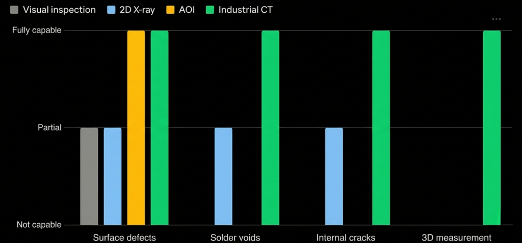
Not all inspection processes are equally valuable. This table provides a comparison of four popular methods according to their effectiveness on the major categories of defects in the inspection process for a power adapter. The comparison clearly highlights the limitations and strengths of each inspection method: visual and AOI inspection (Grey and orange) provide just surface-level information about defects. 2D X-Ray (blue) is more advanced, yet it lacks 3D information capabilities. Only industrial CT (Green) can inspect every type of defect, from surface issues to solder voids and internal cracks.
Transformer Placement & Insulation Clearances
It is the transformer that deals with the voltage transformation between the AC input and DC output; the precise location will dictate the compliance level of the adapter with safety requirements. Using CT helps measure the creepage and clearance values between the primary and secondary windings in compliance with IEC 62368-1 specifications for quality engineers’ reference purposes.
However, without CT, such measurement cannot be accomplished in a sealed and potted adapter.
Hidden Assembly Defects — Cracks, Delamination & Foreign Particles
CT regularly identifies flaws which are induced during the manufacturing process, including hairline cracks from press-fit connections, PCB delamination occurring due to thermal stress, metallic contaminants which can cause intermittent short circuits, and insufficient overmoulding creating pockets of air next to heat-producing parts.
Each of these has an obvious path to failure. Each is invisible using traditional inspection techniques. CT is particularly valuable when conventional inspection methods cannot identify the root cause of a defect, more on this in our post on root cause failure analysis.
Porosity & Voids in Potting Compound
Gaps within potting compounds provide insulating cavities at locations close to heat-emitting components and pose risks of dielectric breakdown around high voltage areas. CT determines the extent, size, and specific position of voids in 3D space, enabling differentiation between uniformly distributed 3% voids and hazardous 3% voids adjacent to the transformer.
The XRAY-LAB Inspection Walkthrough — Step by Step
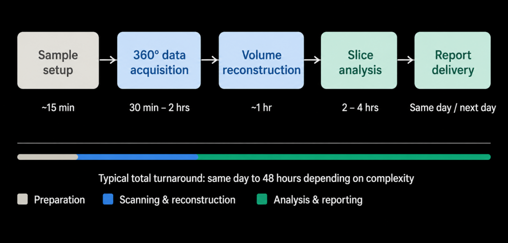
When the specimen arrives at XRAY-LAB, all processes are geared towards achieving a highly detailed internal view of the sample while not physically interacting with the component itself. The adapter is positioned and mounted on the rotational stage exactly as it arrived, no slicing, no disassembly, just straight out of the box, before being rotated through 360° degrees while recording thousands of X-ray projections. These projections undergo reconstruction into a high-resolution 3D volumetric data set, after which the engineer analyzes each slice in three dimensions. Defects, measurements, and standard deviations are carefully identified and documented by the engineer. A detailed report of findings including annotated images and pass/fail decisions is provided.
Why CT Outperforms Other Methods for This Application
2D X-Ray yields a flat projection where components overlap; a void under a component is covered by whatever is sitting on top of it. Fast and effective for an overview, but totally blind to depth.
AOI works great for surface inspection of products on the manufacturing line but it cannot see anything below the surface or inside an encased product.
Cross Sectioning reveals the true inner workings, but only one slice at a time and only after destroying the specimen. The testable object has been destroyed and can’t be tested again, resubmitted, or rescanned.
Industrial Computed Tomography solves all three problems in a single test. Full 3D visualization, scanning of sealed products, and complete preservation of the object. In applications like supplier quality validation or returned parts analysis, where the object will likely need to be resubmitted to the customer, that non-destructive nature is critical. Companies deploying CT as part of incoming and first article programs have consistently noted reduced field returns and reduced warranty issues.
Conclusion
Power adapter failures occur regularly in field applications, but due to the limited scope offered by the testing equipment available to them. Even components that pass all the necessary inspections could have a flaw, be it a fracture, a void, or even misalignment.
CT technology fills this gap.
XRAY LAB always operates on this basic idea: to provide you with a comprehensive view of your product to make informed decisions regarding the approval of any supplier, release of a batch, completion of the PPAP, etc.
Get a CT scan quotation from XRAY-LAB by submitting your sample at: xray-lab.com/en/contact/
Visit the gallery on the official website of XRAY LAB for real x-rays or browse through our full list of industrial CT inspection services.
Frequently Asked Questions
What defects can industrial CT scanning detect in electronics?
Industrially based CT technology can identify solder voids, cold joints, hairline fractures, delamination, contaminants, and porosity within the potting compound without any destruction. This technology identifies flaws that visual inspections, AOI, and 2D X-rays cannot detect.
Is CT scanning destructive to the component being inspected?
CT scanning is completely non-invasive. The adapter or piece is put into the machine, scanned, and completely removed, without any cutting, disassembly, or chemical processing. The same device may undergo another inspection or continue its operation.
How long does an industrial CT inspection take?
Typically, one CT scan of an electric power adapter from the start till completion of all analyses takes from 1/2 to 2 days after samples’ delivery. The process of scanning itself takes 30 minutes to 2 hours, while analysis and reporting take much more time.
When should I use CT inspection instead of 2D X-ray?
Apply CT if you require depth data or 3D measurements. You may use 2D x-ray if a fast overview is needed, but it cannot detect details hidden under other parts or located parallel to the direction of the ray. CT provides the only possibility to detect the internal structure in 3D.
Can CT scanning be used for PPAP and first article inspection?
Yes. CT scanning is more frequently utilized as a component of the PPAP process and FAI as proof that the internal assembly meets spec, not just how it looks from the outside. It is especially important when dealing with sealed parts for which there is no other way to confirm internal dimensions non-destructively.