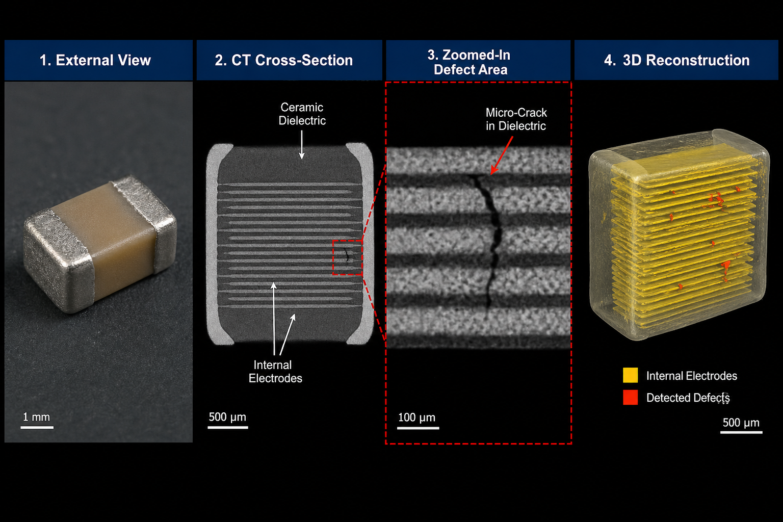
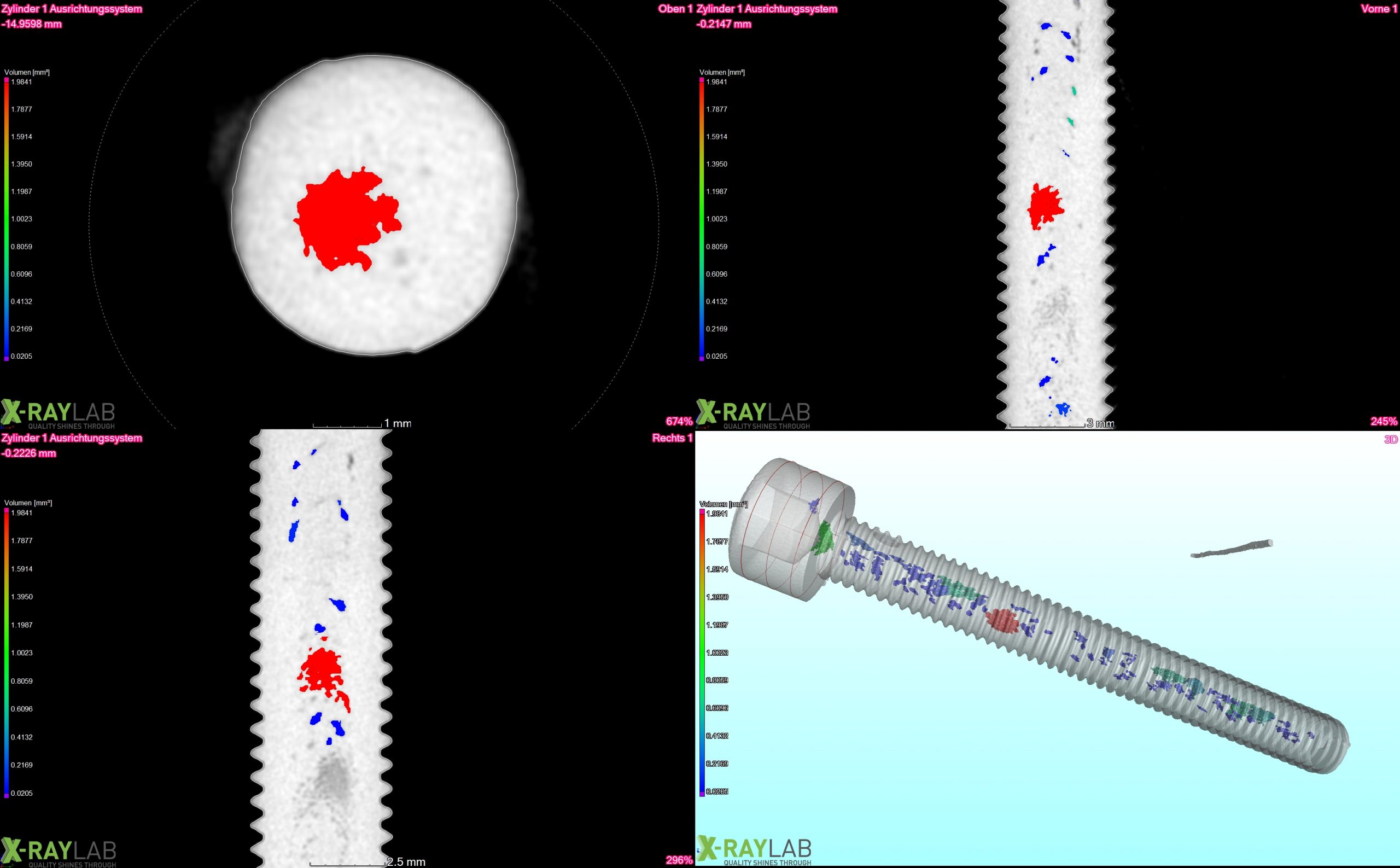
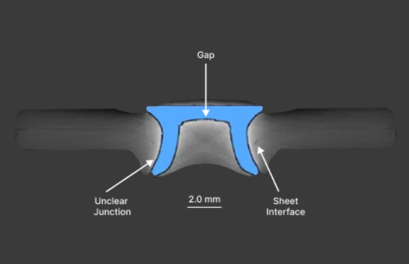
Memory sticks are objects that everybody possesses; they are portable and highly necessary in keeping all important data. However, there are many aspects in memory sticks that are not readily evident.
The solder joints, chips, and connections within these objects might not be immediately visible to the naked eye. It is these solder joints, chips, and connections that determine the efficiency of the memory stick.
It is for this reason that internal quality does matter. Internal quality is extremely significant when manufacturing electronics, and that is where electronics X-ray inspection is applicable.
Why Internal Defects in Electronics Are a Major Risk
The internal defects in electronic gadgets are extremely critical, regardless of their small size. Such defects might go unnoticed by any external observation; however, they are capable of seriously interfering with the functioning of the gadgets.
Common internal defects include:
- Solder voids that weaken electrical connections
- Cracked or cold solder joints that lead to intermittent failures
- Misaligned or improperly placed components
- Hidden PCB trace damage that disrupts signal flow
Defects not only interfere with the working of the gadgets; they also reduce the life span of the products. Even one defect, undetected, could cause premature malfunctioning of the gadgets.
From the manufacturers’ point of view, internal quality assurance is vital not only for better performance but also for good reputation and longevity.
Application Example 1: Memory Devices
Inspection of memory devices such as USB drives poses quite a challenge due to the tiny size of these devices coupled with a lot of components contained within. The connections made are very tight, making space for error very small.
Herein lies the strength of 2D X-ray inspection offered by Xray Lab. The non-disruptive method will make it possible for manufacturers to see the following problems in one glance:
- Poor soldering
- Voids in the solder joints
- Alignment errors of the micro-components
- Chip placements
Unlike other types of inspection that depend on naked eyes, the X-ray process uncovers defects that cannot be seen by naked eyes.
For more complex electronic assemblies, computed tomography (CT) enables deeper internal visualization, improving defect detection in highly compact memory and semiconductor structures.
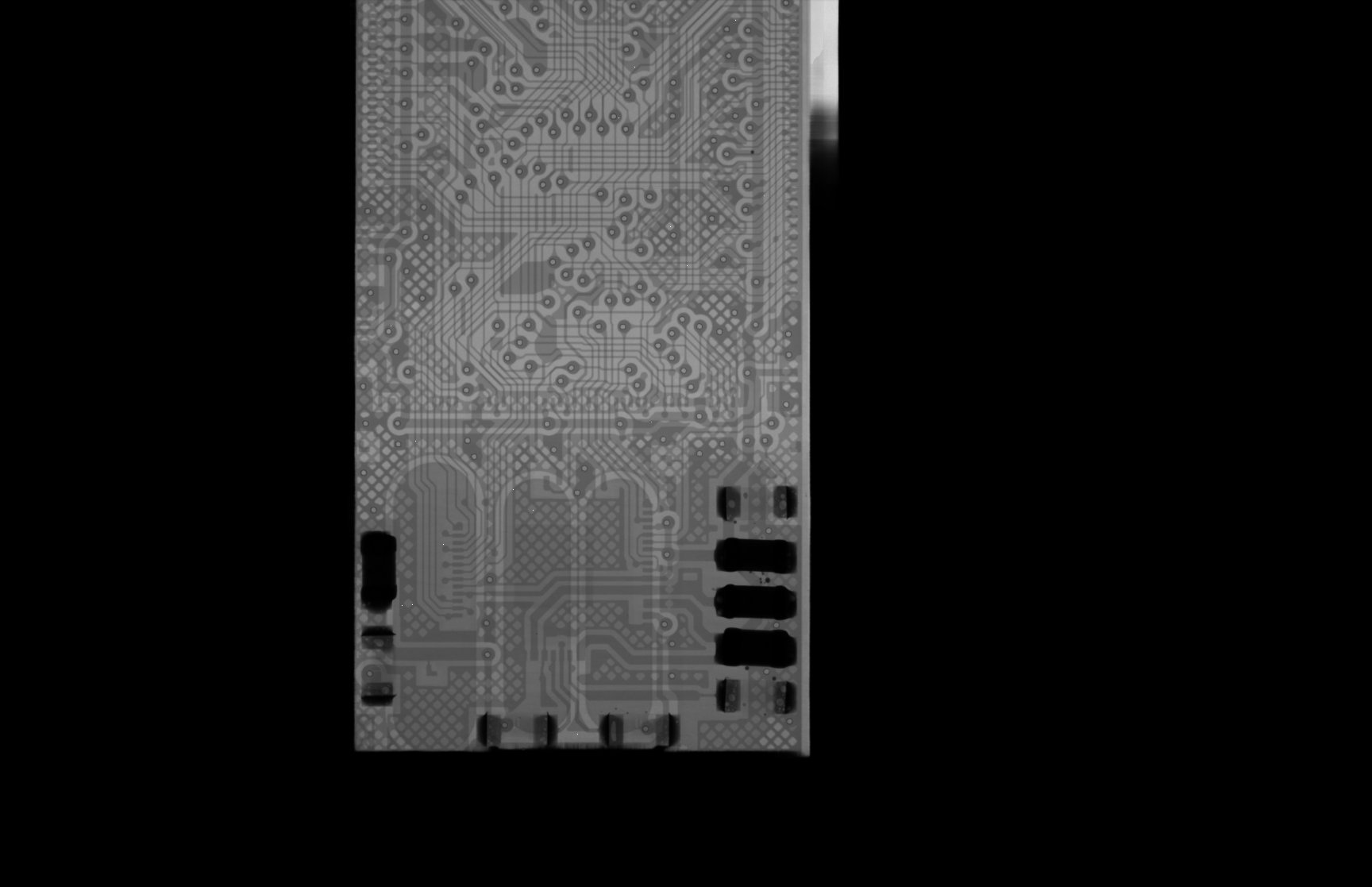
X-ray inspection of a memory device revealing internal chip connections and solder integrity.
Application Example 2: PCB Inspection
Printed Circuit Boards (PCB) form the foundation for today’s electronics, with several components and sophisticated circuits in a small area. It is important to maintain the quality of PCBs.
With Xray Lab’s X-ray inspection systems, manufacturers can inspect PCBs thoroughly without causing any damage. This allows:
- Dense components inspection accurately
- Quality assessment of solder joints through different layers
- Inspection of traces and hidden connectivity issues
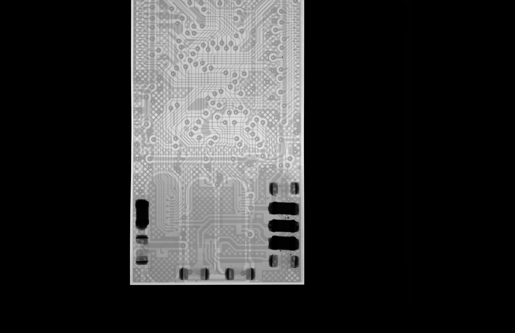
This is further supported by Xray Lab’s microelectronics inspection solutions, where X-ray imaging is used to detect hidden solder joint failures and internal PCB defects that are not visible through optical inspection methods.
The method will ensure that even the most intricate circuit boards can be tested effectively in an efficient manner. It also helps ensure rapid manufacturing cycles without compromising on quality.
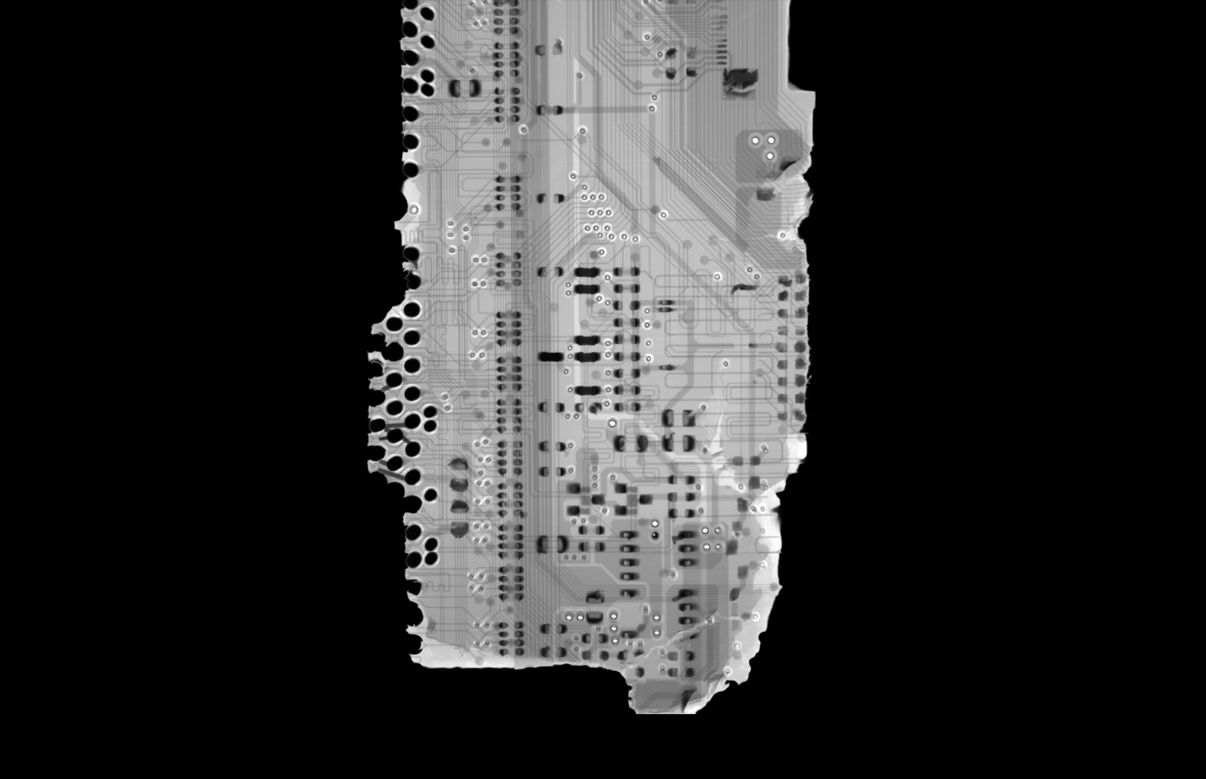
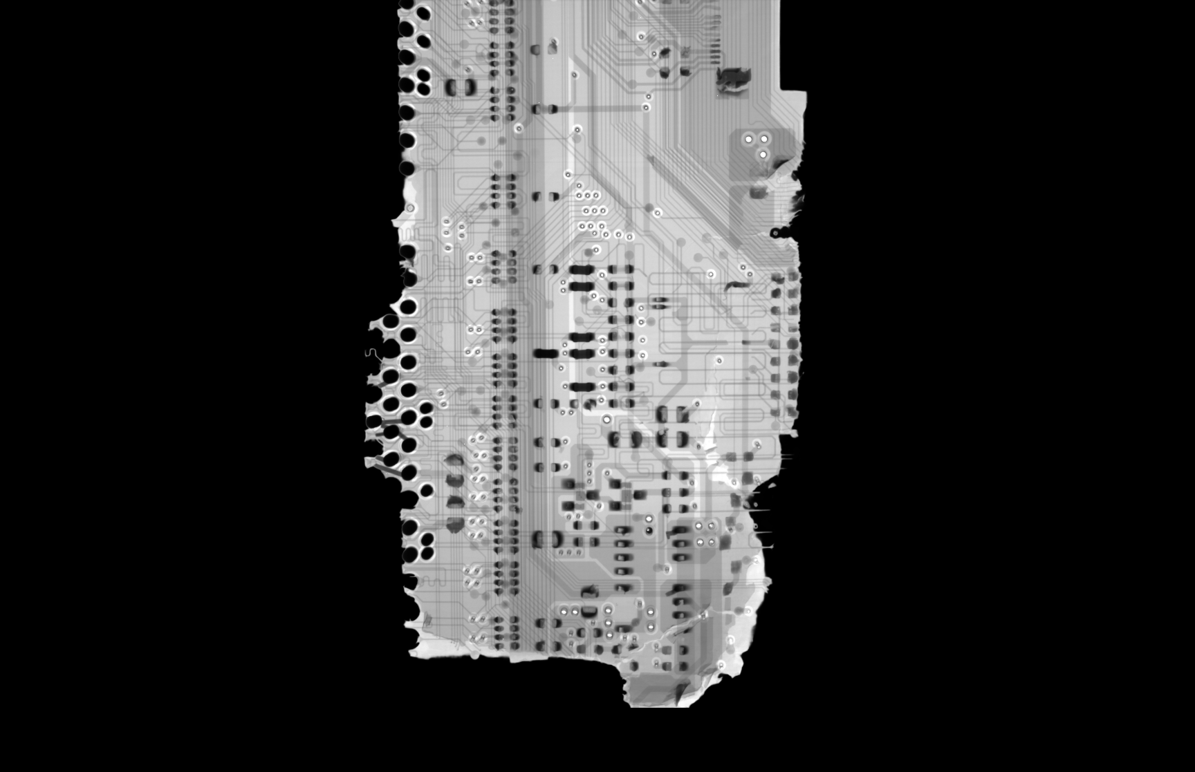
High-resolution X-ray image of a PCB showing component density, solder joints, and internal trace structures.
Key Benefits of Xray Lab’s NDT Solutions
Benefits of X-ray inspection offered by XRAY LAB can be seen in both memory units and printed circuit boards:
- High image resolution ensures precise identification of even minute defects
- Faster inspection processes facilitate efficient production
- Electronics non-destructive testing ensures integrity of components while inspecting them
- Scalability of solutions caters to needs of small production operations as well as large production lines
As highlighted by XRAY LAB, non-destructive testing (NDT) forms the foundation of modern product reliability by ensuring internal defects are detected without damaging the component during inspection.
These benefits allow manufacturers to improve product quality while optimizing efficiency and reducing production costs.
Conclusion
Testing for reliability in electronics doesn’t begin at the surface level; it begins from within.
Internal flaws can negatively impact the performance of electronic products, reduce their lifetime and erode customer trust. This is why internal testing is now an absolute must in the current state of manufacturing.
Manufacturers require high-level visibility to guarantee that every single part conforms to top quality criteria. X-ray testing is a key requirement for every modern electronics manufacturer.
Using non-destructive testing technology, Xray Lab helps electronics manufacturers detect flaws, optimize production and produce reliable electronic products.
Frequently Asked Questions
What Is X-Ray Inspection In Electronics?
X-ray inspection is a non-destructive testing method used to examine the internal structure of electronic components. It helps detect hidden defects such as solder voids, cracks, and misaligned components without damaging the product.
Why Is X-Ray Inspection Important For PCB Quality?
X-ray inspection allows manufacturers to analyze multi-layer PCBs and dense component layouts. It ensures solder joint integrity, detects hidden trace issues, and prevents failures that could impact device performance.
Can X-Ray Inspection Detect Defects In Memory Devices?
Yes, X-ray inspection is highly effective for compact devices like memory sticks. It reveals internal chip connections, solder quality, and structural issues that are not visible through traditional inspection methods.
Is X-Ray Inspection Safe For Electronic Components?
Yes, X-ray inspection is completely non-destructive. It does not affect the functionality or performance of electronic components, making it ideal for quality control during manufacturing.
How Does X-Ray Inspection Improve Manufacturing Efficiency?
By detecting defects early in the production process, X-ray inspection reduces rework, minimizes waste, and improves overall yield. This leads to faster production cycles and cost savings for manufacturers.