CT inspection of ceramic components is redefining how manufacturers approach quality assurance in modern electronics. Ceramic components such as capacitors and resistors are no longer simple passive elements, they are engineered to operate under high voltage, thermal cycling, and miniaturized environments.
Ceramic CT inspection becomes critical in this context because even microscopic internal flaws can disrupt electrical pathways or lead to premature failure. As electronic devices become more compact and performance-driven, the tolerance for hidden defects continues to shrink.
What Makes Ceramic Components So Challenging to Inspect
CT scanning of electronic components addresses a key challenge: ceramics fail internally before they show any external signs. Their brittle structure and layered architecture, especially multilayer ceramic capacitors, make them vulnerable during manufacturing. Micro-cracks in ceramic components can occur in the range of <5-20 µm, requiring high-resolution CT for detection.
Electronic components CT scan methods help uncover issues that originate from:
- Thermal gradients during sintering
- Residual stress accumulation
- Material shrinkage inconsistencies
- Electrode layering imperfections
These factors often lead to micro crack detection in ceramics, internal voids, or density fluctuations that cannot be captured through conventional inspection techniques.
A Closer Look at Micro-CT as a Diagnostic Tool
CT inspection of ceramic components uses micro-CT scanning to generate high-resolution volumetric data of internal structures. This approach goes beyond visualization; it enables precise quantification. Engineers can measure crack length, analyze porosity distribution, and assess density variation with precision.
For applications like CT capacitor inspection, this means:
- Evaluating electrode continuity across layers
- Identifying sub-micron cracks before propagation
- Mapping density gradients that affect dielectric performance
Unlike destructive sectioning, non-destructive testing of ceramics allows repeated inspection of the same component, making it especially valuable for failure analysis and design validation, and it is significantly faster than cross-sectioning.
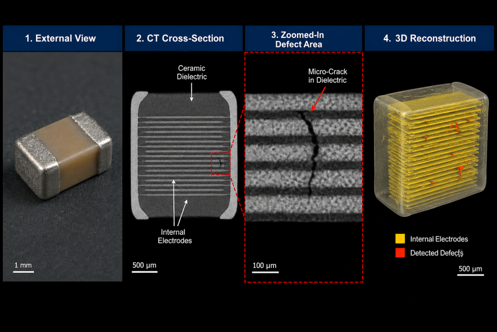
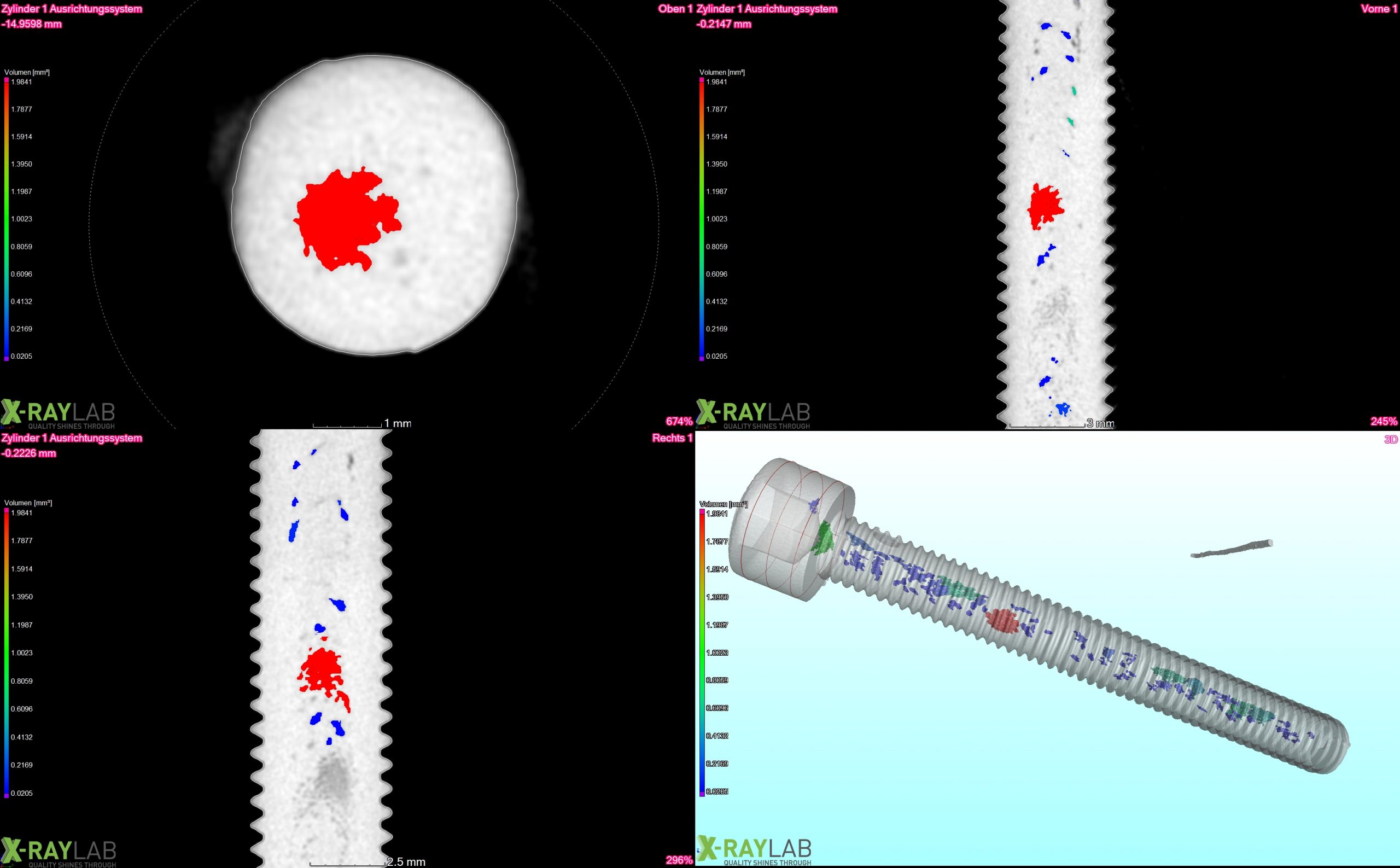
Micro-CT scan of a ceramic capacitor showing cross-section, micro-crack, and 3D internal structure.
From Defect Detection to Root Cause Insight
Electronic components CT scan is not just about finding defects; it’s about understanding why they occur. The 3D datasets produced through CT scanning allow engineers to correlate internal flaws with specific process parameters.
For example:
- A recurring micro-crack pattern may indicate uneven cooling rates
- Localized density variation could point to material mixing inconsistencies
- Voids near electrode interfaces may suggest lamination issues
This level of insight transforms CT ceramic inspection from a quality control tool into a process optimization solution.
Engineering Value in High-Reliability Applications
CT-based inspection of ceramic electronic components plays a decisive role in industries where failure is not an option. Components used in electric vehicles, aerospace systems, and medical electronics must perform consistently under stress.
By integrating non-destructive testing ceramics into production and validation workflows, manufacturers can:
- Detect early-stage defects before assembly
- Improve reliability of mission-critical systems
- Reduce scrap rates and production losses
- Support compliance with strict industry standards
In such environments, CT inspection directly contributes to both safety and cost efficiency.
Adding a Technical Edge: Beyond Visual Inspection
What sets for advanced CT ceramic inspection apart is its ability to move beyond visual assessment into data-driven evaluation. Modern systems can apply grayscale analysis to interpret material density variations, enabling differentiation between fully sintered regions and potential weak zones.
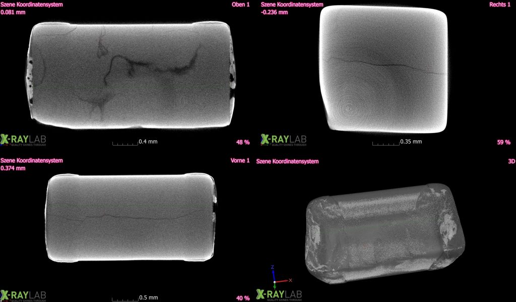
CT scan revealing internal crack propagation in a multilayer ceramic capacitor (MLCC)
Additionally, segmentation techniques allow isolation of specific features, such as electrodes or voids, making it easier to perform targeted analysis. This is particularly useful in CT capacitor inspection, where internal architecture is complex and tightly packed. For the Ceramic capacitor analysis shown, scans were performed at 160 kV and 30 µA, achieving a voxel resolution of approximately 1.7 µm using approximately 2400 projections over 360°. With a magnification of approximately 56× and a high-resolution flat panel detector, this setup enabled clear visualization of internal electrode layers and micro-crack features. This enables detailed visualization of electrode layers, detection of micro-cracks, and analysis of internal structural consistency.
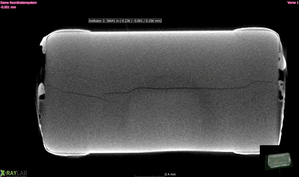
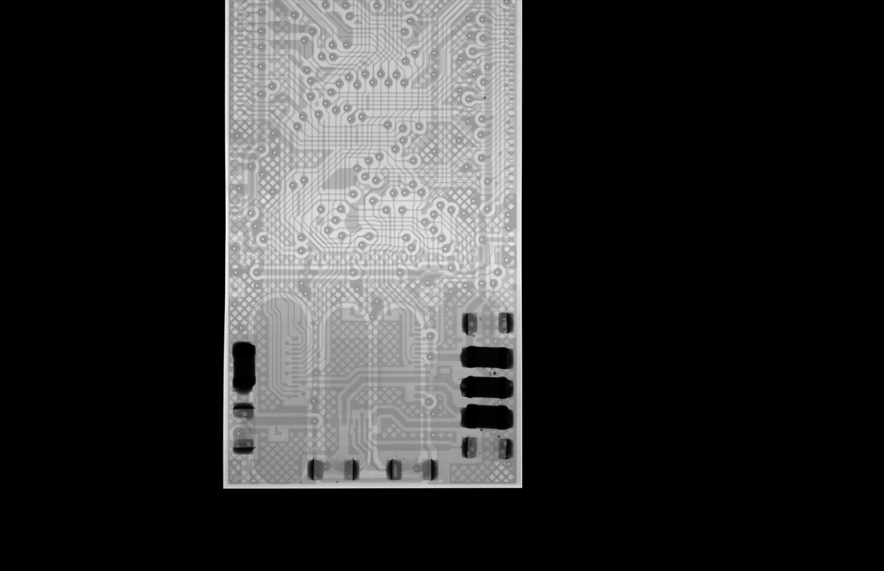
X-ray CT slice showing subsurface crack in a ceramic capacitor
This CT slice of a ceramic capacitor shows a subsurface internal crack appearing as a dark line due to density differences. The crack runs horizontally through the ceramic, caused by mechanical stress such as board flexing or thermal cycling. The 3D inset helps visualize its position and extent within the component.
These capabilities elevate CT scan of electronic components from a diagnostic method to an engineering intelligence tool.
Conclusion
CT-based inspection of ceramic electronic components is no longer just an advanced option—it is becoming a necessity in precision electronics manufacturing. As ceramic components evolve in complexity and application of criticality, the ability to inspect them internally without damage provides a clear competitive advantage.
This is where XRAY LAB plays a crucial role. By combining advanced micro-CT systems with application-specific expertise, XRAY LAB helps manufacturers move beyond simple defect detection toward actionable engineering insights. Instead of just identifying flaws, XRAY LAB enables teams to understand failure mechanisms, optimize manufacturing parameters, and improve overall product design. This approach supports zero defect manufacturing by enabling early detection of internal defects before they impact performance.
Through high-resolution electronic components CT scan capabilities, Xray Lab supports:
- Accurate micro crack detection in ceramics at early stages
- Detailed analysis for CT capacitor inspection and multilayer structures
- Data-driven quality control using non-destructive testing ceramics
- Faster decision-making in R&D, production, and failure analysis
In a landscape where even, microscopic imperfections can impact performance, XRAY LAB provides the clarity, precision, and confidence needed to ensure ceramic components meet the highest reliability standards.
Frequently Asked Questions
What is CT ceramic inspection used for?
CT ceramic inspection is used to analyze the internal structure of ceramic electronic components and detect defects like cracks, voids, and density variations without damaging them.
How does micro crack detection in ceramics improve reliability?
Micro crack detection in ceramics helps identify early-stage structural weaknesses that could expand under stress and cause component failure.
Why is CT capacitor inspection important?
CT capacitor inspection ensures that internal electrode layers and dielectric materials are properly aligned and free from defects, which is essential for performance and safety.
Can CT scanning measure material density in ceramics?
Yes, electronic components CT scan systems can analyze grayscale values to detect density variations and material inconsistencies.
Which industries rely on non destructive testing ceramics?
Industries such as automotive, aerospace, consumer electronics, and medical devices rely on non destructive testing ceramics to ensure product reliability.