The exterior appearance of an LED bulb may seem to be an easily discernible electronic part. Small casing, drivers, LEDs, and a cooling mechanism packed together in one unit.
However, inside an LED bulb resides a sophisticated system of electronics that influences directly:
- Lifetime
- Heat dissipation
- Electrical integrity
- Efficiency
- Safety
In many cases, the majority of defects of the most critical nature that exist in the LED package remain hidden from human eyesight. Voided solder joints, broken leads, misplaced components, thermal damage, and any other issues connected with the manufacturing process can remain undetected until the product fails.
It is precisely the explanation for why many organizations nowadays prefer turning to CT scanning and x-ray analysis.
The use of industrial computed tomography gives engineers the opportunity to examine the complete inner structure of the LED bulb without having to open it up.
Learn about this type of inspection technology in this article: What Is Industrial CT Scanning? A Comprehensive Guide for Manufacturers. For the electronics industry, CT analysis delivers more in-depth insights compared to conventional approaches. The design of the LED bulb might seem quite an uncomplicated electronic component at first glance. Small casing, driver, LED lights, and cooling system combined in one assembly.
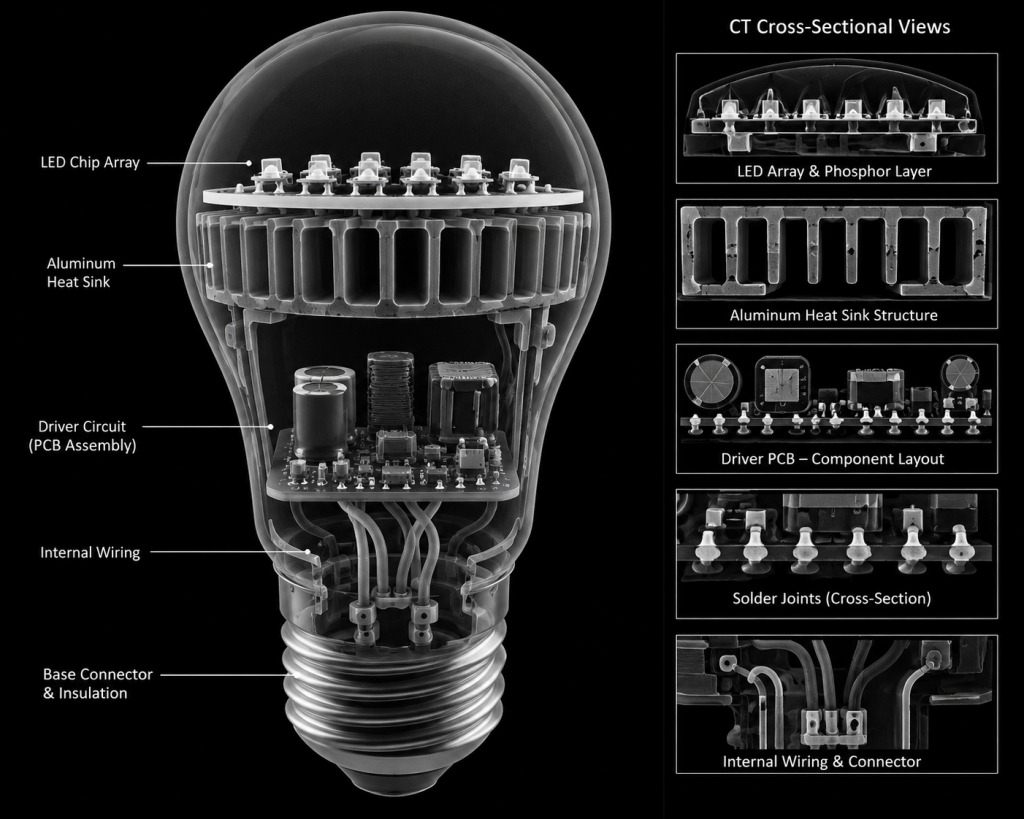
Industrial CT scan revealing the complete internal architecture of an LED bulb, including driver electronics, solder joints, LED array, and thermal management structure in a non-destructive 3D view.
Why LED Bulb X-Ray Inspection Matters
LED components are designed to function consistently for thousands of hours through thermal and electrical stress.
Even minor internal defects can lead to:
- Flickering
- Reduced brightness
- Thermal degradation
- Premature driver failure
- Intermittent electrical behavior
- Complete product failure
Destructive testing, common with traditional inspection procedures, can only provide partial results on one particular sample.
By using industrial CT electronic inspection, this problem is solved since this procedure allows one to digitally examine all components of the assembled part.
This makes CT scan LED assembly analysis valuable for:
- Product development
- Manufacturing validation
- Supplier quality control
- Failure investigation
- Assembly verification
- Process optimization
What Industrial CT Can Reveal Inside an LED Bulb
Driver Electronics Inspection
One of the major weak points in LED bulbs is the driver circuit.
Driver circuits are responsible for regulating the current and converting input power to electrical energy for the LEDs. Inefficiencies in component arrangement or heat damage will greatly affect the longevity of the product.
Industrial CT scanning allows engineers to inspect:
- Capacitor placement
- PCB assembly quality
- Component alignment
- Internal wiring
- Solder joints
- Cracked traces
- Voids beneath components
Unlike conventional optical inspection, CT imaging reveals hidden defects beneath the PCB surface and inside dense assemblies.
Related high-precision inspection techniques are detailed in X-ray Inspection of Microelectronics and PCB Defect Detection
In modern LED devices when miniaturization keeps increasing, this kind of test helps understand the manufacturing process and future reliability.
When it comes to compact LED devices that have limited space, then CT scanning is especially important since there are places that cannot be inspected otherwise.
At XRAY-LAB, industrial CT solutions help electronics manufacturers analyze miniature assemblies with high-resolution non-destructive inspection capabilities.
Solder Quality Analysis Using CT Scanning
Solder integrity directly impacts LED reliability.
Defective solder joints may initially function correctly but fail later due to thermal cycling, vibration, or electrical stress.
Industrial CT scanning can detect:
- Solder voids
- Cold solder joints
- Insufficient solder
- Cracks
- Bridging defects
- Incomplete wetting
This becomes more important in the case of LED driver boards due to the compactness leading to higher concentrations of heat.
The use of CT scan for analysis of an LED assembly helps in identifying defects along with determining their dimensions and severity.
It is hard to get this type of information using conventional 2D inspections.
Heat Dissipation Structures and Thermal Design Verification
Heat is one of the biggest factors affecting LED lifespan.
Most LED bulbs include internal heat dissipation structures such as:
- Aluminum heat sinks
- Thermal pads
- Cooling fins
- Conductive interface materials
If thermal transfer is inefficient, internal temperatures rise rapidly and accelerate component degradation.
Industrial CT electronics inspection helps manufacturers evaluate:
- Heat sink positioning
- Thermal interface contact
- Air gaps
- Material distribution
- Structural consistency
CT imaging can also reveal assembly defects that disrupt heat flow pathways inside compact LED housings.
For high-performance lighting products, thermal verification is a critical part of quality assurance.
Assembly Verification in Compact LED Designs
Modern LED bulbs are highly compact and densely integrated.
Manufacturers must ensure accurate alignment of:
- PCBs
- Connectors
- LED arrays
- Internal supports
- Driver modules
- Diffuser components
Even small assembly deviations can create electrical instability or mechanical stress.
Industrial CT scanning enables full internal assembly verification without disassembling the product.
Engineers can analyze:
- Internal positioning
- Mechanical clearances
- Structural integrity
- Fastener placement
- Connector seating
- Cable routing
This is especially useful during product development and first article inspection.
XRAY-LAB supports electronics manufacturers with industrial CT systems capable of high-detail inspection for miniature and densely packed electronic assemblies.
LED Bulb Failure Analysis Using Industrial CT
Failure analysis is one of the most powerful applications of CT scanning.
When LED products fail in the field, manufacturers need to identify the root cause quickly and accurately.
Industrial CT helps engineers investigate:
- Burned components
- Thermal damage
- Broken internal connections
- Structural cracks
- Driver failures
- Delamination
- Material degradation
Because CT scanning is non-destructive, failed components can be analyzed while preserving their original condition.
This allows engineers to examine defect propagation and internal damage pathways in greater detail than destructive teardown methods.
In many cases, CT inspection reduces investigation time while improving diagnostic accuracy.
Why CT Scanning Is Valuable for Electronics Manufacturing
Electronics assemblies continue becoming smaller, denser, and more complex.
As miniaturization increases, hidden internal defects become more difficult to detect using conventional inspection methods.
Industrial CT electronics inspection offers several major advantages:
Inspection Capability | Traditional Inspection | Industrial CT Scanning |
Internal Defect Detection | Limited | Excellent |
Non-Destructive Analysis | Partial | Full |
3D Visualization | No | Yes |
Hidden Solder Inspection | Limited | High Accuracy |
Assembly Verification | Partial | Complete |
Failure Analysis Depth | Moderate | Advanced |
For manufacturers focused on reliability and quality assurance, CT scanning provides significantly deeper visibility into electronic assemblies.
How XRAY-LAB Supports Electronics CT Inspection
XRAY-LAB provides advanced industrial CT and X-ray inspection solutions for electronics and miniature assemblies.
The company supports manufacturers with:
- Industrial CT electronics inspection
- LED bulb X-ray inspection
- High-resolution defect analysis
- Solder inspection
- PCB inspection
- Failure analysis
- Non-destructive testing
- Assembly verification
- AI-assisted defect detection
With expertise in industrial X-ray and CT technologies, XRAY-LAB helps electronics manufacturers improve quality control, identify hidden defects, and optimize production reliability.
Frequently Asked Questions
What Is LED Bulb X-Ray Inspection?
LED bulb X-ray inspection is a non-destructive testing method used to inspect internal electronic structures, solder joints, and assembly quality inside LED products.
Can CT Scanning Detect Solder Defects in LED Assemblies?
Yes. Industrial CT scanning can identify solder voids, cracks, cold joints, bridging defects, and insufficient solder inside LED driver electronics.
Why Is CT Inspection Important for Electronics Manufacturing?
CT inspection helps manufacturers detect hidden internal defects that cannot be identified through visual inspection or conventional testing methods.
What Can a CT Scan Reveal Inside an LED Bulb?
A CT scan can reveal internal driver electronics, solder quality, heat dissipation structures, connector positioning, cracks, voids, and assembly defects.
Is Industrial CT Scanning Non-Destructive?
Yes. Industrial CT scanning allows complete internal inspection without opening or damaging the LED assembly.