Printed Circuit Boards (PCBs) are the backbone of every modern electronic device, from smartphones to medical instruments, automotive systems to industrial controllers. As PCB complexity increases with miniaturization and high‑density interconnects, traditional inspection methods like visual or optical testing fall short. X‑Ray inspection of microelectronics provides the deep, non‑destructive insight that manufacturers need to detect hidden defects in PCB assemblies and ensure product reliability.
Table of Contents
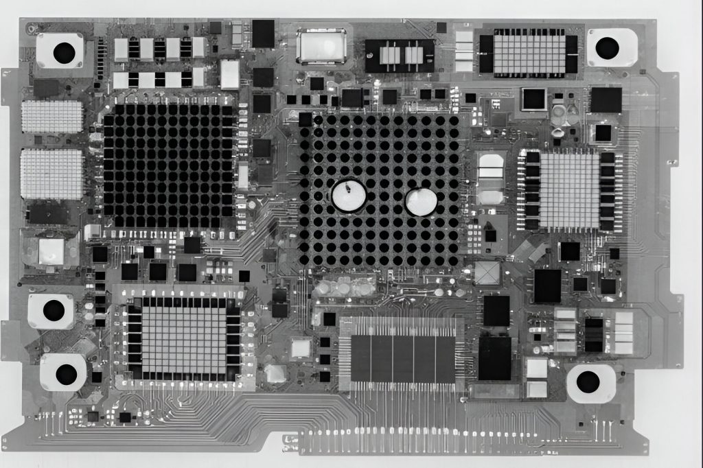
High-resolution X-ray scan of a PCB assembly revealing internal solder joints, BGA connections, and hidden voids detected through X-RAYLAB’s advanced microelectronics inspection services.
What Is X Ray Inspection in Microelectronics?
X‑Ray inspection uses high‑energy electromagnetic radiation to penetrate assembled PCBs and produce detailed internal images. Unlike optical inspection, which only reveals surface features, X‑Ray systems can visualize:
- Internal solder joints
- Hidden interconnects under Ball Grid Arrays (BGAs) and Chip‑Scale Packages (CSPs)
- Multi‑layer board features
- Voids, cracks, and delaminations within components
Because X‑Rays can reveal what’s inside complex assemblies without damaging the board, this method is critical for high‑reliability applications in aerospace, automotive, medical, and consumer electronics.
How X Ray Inspection Works
In microelectronics inspection, an X‑Ray source emits radiation through the PCB assembly. A detector on the opposite side captures the attenuated X‑Rays and generates a grayscale image based on material density differences. Denser materials like solder and copper appear brighter, while voids or air gaps appear darker.
There are two main types of X‑Ray inspection systems used in PCB assembly:
- 2D X‑Ray Inspection
2D systems capture a planar projection of the internal structure. They are fast and cost‑effective, and ideal for:
- Through‑Hole solder inspection
- Basic BGA joint verification
- Detecting large voids or misalignments
However, 2D X‑Rays can suffer from image overlap when multiple features are stacked, making interpretation difficult in dense boards.
- 3D X‑Ray / Computed Tomography (CT)
3D X‑Ray CT rotates the PCB and reconstructs a volumetric image from many angles. This allows for:
- Precise measurement of void volumes
- Localization of cracks within solder balls
- Layer‑by‑layer analysis of complex packages
3D CT delivers the most comprehensive insight, especially for advanced microelectronics with fine pitches and hidden interconnects.
X-RAYLAB supports electronics manufacturers by providing specialized X-ray inspection services for PCB assemblies, enabling the detection of internal defects that cannot be identified through visual or optical inspection methods. By using advanced 2D and 3D X-ray technologies, X-RAYLAB delivers clear insight into the internal structure of complex microelectronic assemblies.
Common Hidden Defects in PCB Assemblies
X‑Ray inspection is particularly effective at revealing defects that cannot be detected by other inspection methods:
Voids in Solder Joints: Voids are air pockets that form during solder reflow. Excessive voiding weakens joints and can cause thermal and mechanical failures.
Insufficient or Excess Solder: Too little solder can lead to open circuits, while too much solder can create shorts or bridging between pads.
Misalignment and Tombstoning: Fine‑pitch components can shift during assembly. Tombstoning is when one end of a component lifts off the pad entirely.
Cracks and Fractures: Mechanical stress or manufacturing defects can produce cracks in solder joints or component bodies.
Delamination and Material Separation: Layers within the PCB can separate due to moisture or thermal cycling — a hidden reliability risk.
Benefits of X Ray Inspection for PCB Quality
Non‑Destructive and Fast: X‑Ray inspection allows manufacturers to inspect entire assemblies without cutting or cross‑sectioning, preserving the board for further testing or shipment.
High Detection Accuracy: With advanced imaging and automated defect recognition software, X‑Ray systems detect defects with high precision.
Supports Process Optimization: By analyzing defect trends, manufacturers can optimize solder paste printing, component placement, and reflow profiles to reduce yield loss.
Compliance and Traceability: Many industries require documented quality inspections. X‑Ray data can be archived for traceability and compliance reporting.
X-RAYLAB’s Approach to Microelectronics Inspection
At X-RAYLAB, we combine state‑of‑the‑art X‑Ray and CT inspection platforms with expert analysis to deliver actionable insights for your PCB assemblies. Our services include:
- High‑resolution 2D and 3D imaging
- Automated defect detection algorithms
- Quantitative void and solder volume analysis
- Comprehensive inspection reports
Whether you’re troubleshooting yield issues or qualifying new designs, X-RAYLAB’s microelectronics inspection services help you detect hidden defects early and reliably.
Frequently Asked Questions
What Is The Main Purpose Of X Ray Inspection In PCBs?
X‑Ray inspection identifies internal defects like voids, misalignment, and soldering issues in PCBs that are invisible to optical inspection.
How Does X Ray Inspection Improve PCB Assembly Quality?
By revealing hidden defects early, X‑Ray inspection enables process optimization, reduces failure rates, and improves product reliability.
What Is The Difference Between 2D X Ray And 3D CT Inspection?
2D X‑Ray provides planar images, while 3D CT reconstructs volumetric data for more detailed analysis of complex internal features.
Can X Ray Inspection Damage Electronics?
No — X‑Ray inspection is non‑destructive and safe for PCB assemblies when performed by trained professionals.
Which Industries Benefit Most From X Ray PCB Inspection?
Aerospace, automotive, medical devices, and advanced consumer electronics — wherever high reliability is essential.
